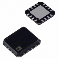
ADN2891ACPZ-WP Analog Devices Inc, ADN2891ACPZ-WP Datasheet

ADN2891ACPZ-WP
Specifications of ADN2891ACPZ-WP
Related parts for ADN2891ACPZ-WP
ADN2891ACPZ-WP Summary of contents
Page 1
FEATURES Input sensitivity p rise/fall times CML outputs: 700 mV p-p differential Programmable LOS detector: 3 signal strength indicator (RSSI) SFF-8472-compliant average power measurement Single-supply operation: 3.3 V Low power dissipation: ...
Page 2
ADN2891 TABLE OF CONTENTS Specifications..................................................................................... 3 Absolute Maximum Ratings............................................................ 5 Thermal Resistance ...................................................................... 5 ESD Caution.................................................................................. 5 Pin Configuration and Function Descriptions............................. 6 Typical Performance Characteristics ............................................. 7 Theory of Operation ...................................................................... 10 Limiting Amplifier ..................................................................... 10 REVISION HISTORY 7/05—Rev. ...
Page 3
SPECIFICATIONS Test Conditions: VCC = 2 3.6 V, VEE = Table 1. Parameter Min QUANTIZER DC CHARACTERISTICS Input Voltage Range 1.8 Input Common Mode 2.1 Differential Input Range Differential Input Sensitivity 5.2 Input Offset Voltage ...
Page 4
ADN2891 Parameter Min LOGIC INPUTS (SQUELCH Input High Voltage 2 Input Low Voltage IL Input Current LOGIC OUTPUTS (LOS Output High Voltage 2 Output Low Voltage OL Typ Max Unit ...
Page 5
ABSOLUTE MAXIMUM RATINGS Table 2. Parameter Power Supply Voltage Minimum Voltage (All Inputs and Outputs) Maximum Voltage (All Inputs and Outputs) Storage Temperature Operating Temperature Range Production Soldering Temperature Junction Temperature ESD CAUTION ESD (electrostatic discharge) sensitive device. Electrostatic charges ...
Page 6
ADN2891 PIN CONFIGURATION AND FUNCTION DESCRIPTIONS Note that the LFCSP has an exposed pad on the bottom. To improve heat dissipation, the exposed pad must be soldered to the GND plane with filled vias. Table 4. Pin Function Descriptions Pin ...
Page 7
TYPICAL PERFORMANCE CHARACTERISTICS 50ps/DIV Figure 3. Eye of ADN2891 @ 25°C, 3.2 Gbps, and 10 mV Input 50ps/DIV Figure 4. Eye of ADN2891 @ 25°C, 3.2 Gbps, and 500 mV Input 50ps/DIV Figure 5. Eye of ADN2891 @ 95°C, 3.2 ...
Page 8
ADN2891 70 60 –40°C 50 +95°C +25°C 40 +95°C 30 +25°C DEASSERTION 20 –40°C 10 ASSERTION 0 1k 10k R (Ω) TH Figure 8. LOS Trip and Release vs 10k R (Ω) TH ...
Page 9
PD_CATHODE CURRENT (PHOTODIODE CURRENT) (μA) Figure 14. RSSI Output vs. Average Photodiode Current PD_CATHODE CURRENT (PHOTODIODE ...
Page 10
ADN2891 THEORY OF OPERATION LIMITING AMPLIFIER Input Buffer The ADN2891 limiting amplifier provides differential inputs (PIN/NIN), each having single-ended, on-chip, 50 Ω termina- tion. The amplifier can accept either dc-coupled or ac-coupled signals; however, an ac-coupled signal is recommended. Using ...
Page 11
APPLICATIONS PCB DESIGN GUIDELINES Proper RF PCB design techniques must be used to ensure optimal performance. Output Buffer Power Supply and Ground Planes Pin 9 (DRVEE) and Pin 12 (DRVCC) are the power supply and ground pins that provide current ...
Page 12
ADN2891 PCB Layout Figure 21 shows the recommended PCB layout. The 50 Ω transmission lines are the traces that bring the high frequency input and output signals (PIN, NIN, OUTP, and OUTN) to the SMA connectors with minimum reflection. To ...
Page 13
... MAX 0.90 0.85 0.80 SEATING PLANE ORDERING GUIDE Model Temperature Range ADN2891ACPZ-500RL7 1 –40°C to +95°C 1 ADN2891ACPZ-RL7 –40°C to +95°C ADN2891ACPZ-RL 1 –40°C to +95°C EVAL-ADN2891EB Pb-free part. 3.00 0.60 MAX BSC SQ 0.45 2.75 TOP BSC SQ VIEW 0.50 BSC 1 ...
Page 14
ADN2891 NOTES Rev Page ...
Page 15
NOTES Rev Page ADN2891 ...
Page 16
ADN2891 NOTES © 2005 Analog Devices, Inc. All rights reserved. Trademarks and registered trademarks are the property of their respective owners. D05244–0–7/05(A) Rev Page ...


