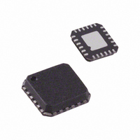
ADN8810ACPZ Analog Devices Inc, ADN8810ACPZ Datasheet

ADN8810ACPZ
Specifications of ADN8810ACPZ
Available stocks
Related parts for ADN8810ACPZ
ADN8810ACPZ Summary of contents
Page 1
FEATURES High precision 12-bit current source Low noise Long term stability Current output from 300 mA Output fault indication Low drift Programmable maximum current 24-lead 4 mm × leadframe chip scale package 3-wire serial interface ...
Page 2
ADN8810 TABLE OF CONTENTS ADN8810–Specifications ................................................................ 3 Timing Characteristics ..................................................................... 5 Absolute Maximum Ratings ............................................................ 6 ESD Caution .................................................................................. 6 Pin Configuration and Function Descriptions ............................. 7 ADN8810 Terminology ................................................................... 8 Typical Performance Characteristics ............................................. 9 Functional Description .................................................................. 11 ...
Page 3
ADN8810–SPECIFICATIONS Table 1. Electrical Characteristics (AVDD = DVDD = 5 V, PVDD = 3.3 V, AVSS = DVSS = DGND = 0 V, TA= 25°C, covering IOUT from 2% IFS to 100% IFS, unless otherwise noted.) Parameter DC PERFORMANCE Resolution ...
Page 4
ADN8810 Parameter INTERFACE TIMING 2 Clock Frequency RESET Pulsewidth NOTES 1 With respect to AVSS. 2 See Timing Characteristics for timing specifications Ω SN Symbol Condition f CLK t 11 Rev Page 4 of ...
Page 5
TIMING CHARACTERISTICS Table 2. Timing Characteristics Parameter Description f SCLK Frequency CLK t SCLK Cycle Time 1 t SCLK Width High 2 t SCLK Width Low Low to SCLK High Setup High to SCLK ...
Page 6
ADN8810 ABSOLUTE MAXIMUM RATINGS Table 3. ADN8810 Absolute Maximum Ratings Parameter Supply Voltage Input Voltage Output Short-Circuit Duration to GND Storage Temperature Range Operating Temperature Range Junction Temperature Range CP Package ESD CAUTION ESD (electrostatic discharge) sensitive device. Electrostatic charges ...
Page 7
PIN CONFIGURATION AND FUNCTION DESCRIPTIONS Table 4. Pin Function Description Pin No. Mnemonic Type 1 ADDR2 Digital Input 2 RSN Analog Input 3 FB Analog Input 4 ADDR1 Digital Input 5 ADDR0 Digital Input 6 FAULT Digital Output 7 SB ...
Page 8
ADN8810 ADN8810 TERMINOLOGY Relative Accuracy Relative accuracy or integral nonlinearity (INL measure of the maximum deviation, in least significant bits (LSBs), from an ideal line passing through the endpoints of the DAC transfer function. Figure 5 shows a ...
Page 9
TYPICAL PERFORMANCE CHARACTERISTICS 1.2 1.0 0.8 0.6 0.4 0.2 0 –0.2 –0.4 –0.6 –0.8 0 500 1,000 1,500 2,000 2,500 3,000 3,500 4,000 CODE Figure 5. Typical INL Plot 0.4 0.3 0.2 0.1 0 –0.1 –0.2 –0.3 0 500 1,000 ...
Page 10
ADN8810 0.50 CODE = x000 0.45 0.40 0.35 0.30 0.25 0.20 0.15 0.10 0.05 0 –40 –15 10 TEMPERATURE (°C) Figure 11. PVDD Supply Current vs. Temperature 12 CODE = x000 –40 –15 10 ...
Page 11
FUNCTIONAL DESCRIPTION The ADN8810 is a single 12-bit current output D/A converter with a 3-wire SPI interface eight devices can be independently programmed from the same SPI bus. The full-scale output current is set with two external resistors. ...
Page 12
ADN8810 DAC to be updated eight ADN8810 devices with unique addresses can be driven from the same serial data bus. Table 5 shows how the 16-bit DATA input word is divided into an address byte and a data ...
Page 13
R2 1.62kΩ 1µF 1.62kΩ DITHER 4.096V AD8605 Figure 19. Adding Dither to the Reference Voltage Set the gain of the dither by adjusting the ratio R1. Increase C to lower the cutoff frequency of ...
Page 14
ADN8810 POWER SUPPLY OTHER 5V DIGITAL LOGIC LOGIC GROUND RETURN DVDD AVDD PVDD DVSS DGND ADN8810 Figure 23. Star Supply and Ground Technique To improve thermal dissipation, the slug on the bottom of the LFCSP package should ...
Page 15
... SEATING PLANE ORDERING GUIDE Model Temperature Range ADN8810ACP –40°C to +85°C ADN8810ACP-REEL7 –40°C to +85°C ADN8810ACPZ 1 –40°C to +85°C ADN8810ACPZ-REEL7 1 –40°C to +85° RoHS Compliant Part. 0.60 MAX 4.00 BSC SQ 0.60 MAX 19 18 0.50 BSC TOP 3 ...
Page 16
ADN8810 NOTES ©2004–2009 Analog Devices, Inc. All rights reserved. Trademarks and registered trademarks are the property of their respective owners. D03195-0-4/09(A) Rev Page ...


