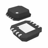
ADP3334ACPZ-REEL7 Analog Devices Inc, ADP3334ACPZ-REEL7 Datasheet - Page 3

ADP3334ACPZ-REEL7
Manufacturer Part Number
ADP3334ACPZ-REEL7
Description
IC,VOLT REGULATOR,ADJUSTABLE,+1.5 TO +10V,BIPOLAR,LLCC,8PIN,PLASTIC
Manufacturer
Analog Devices Inc
Series
anyCAP®r
Datasheet
1.ADP3334ACPZ-REEL7.pdf
(12 pages)
Specifications of ADP3334ACPZ-REEL7
Package / Case
8-LFCSP
Mounting Type
Surface Mount
Current - Output
500mA
Voltage - Output
1.5 ~ 10 V
Voltage - Input
2.6 ~ 11 V
Operating Temperature
-40°C ~ 85°C
Regulator Topology
Positive Adjustable
Voltage - Dropout (typical)
0.2V @ 500mA
Number Of Regulators
1
Lead Free Status / RoHS Status
Lead free / RoHS Compliant
Current - Limit (min)
-
Lead Free Status / RoHS Status
Lead free / RoHS Compliant
Available stocks
Company
Part Number
Manufacturer
Quantity
Price
Company:
Part Number:
ADP3334ACPZ-REEL7
Manufacturer:
SEIKO
Quantity:
40 000
Part Number:
ADP3334ACPZ-REEL7
Manufacturer:
ADI/亚德诺
Quantity:
20 000
ABSOLUTE MAXIMUM RATSINGS*
Input Supply Voltage . . . . . . . . . . . . . . . . . . . –0.3 V to +16 V
Shutdown Input Voltage . . . . . . . . . . . . . . . . –0.3 V to +16 V
Power Dissipation . . . . . . . . . . . . . . . . . . . . Internally Limited
Operating Ambient Temperature Range . . . . –40°C to +85°C
Operating Junction Temperature Range . . . –40°C to +150°C
Storage Temperature Range . . . . . . . . . . . . –65°C to +150°C
Lead Temperature Range (Soldering 6 sec) . . . . . . . . . . 300°C
*Stresses above those listed under Absolute Maximum Ratings may cause perma-
CAUTION
ESD (electrostatic discharge) sensitive device. Electrostatic charges as high as 4000 V readily
accumulate on the human body and test equipment and can discharge without detection. Although
the ADP3334 features proprietary ESD protection circuitry, permanent damage may occur on
devices subjected to high energy electrostatic discharges. Therefore, proper ESD precautions are
recommended to avoid performance degradation or loss of functionality.
REV. B
nent damage to the device. This is a stress rating only. Functional operation of the
device at these or any other conditions above those listed in the operational
sections of this specification is not implied. Exposure to absolute maximum rating
conditions for extended periods may affect device reliability.
JA
JA
JA
JA
JA
JA
4-Layer SOIC-8 . . . . . . . . . . . . . . . . . . . . . . . . . 86.6°C/W
4-Layer LFCSP-8 . . . . . . . . . . . . . . . . . . . . . . . . . . 48°C/W
4-Layer MSOP-8 . . . . . . . . . . . . . . . . . . . . . . . . . 158°C/W
2-Layer SOIC-8 . . . . . . . . . . . . . . . . . . . . . . . . 122.3°C/W
2-Layer LFCSP-8 . . . . . . . . . . . . . . . . . . . . . . . . . . 62°C/W
2-Layer MSOP-8 . . . . . . . . . . . . . . . . . . . . . . . . . 220°C/W
OUT
OUT
NC
FB
1
2
3
4
NC = NO CONNECT
ADP3334ARM
Model
ADP3334AR
ADP3334ACP
ADP3334ARM
(Not to Scale)
TOP VIEW
8
7
6
5
IN
IN
SD
GND
ADJ
ADJ
ADJ
Output Description
PIN CONFIGURATIONS
Standard Small Outline
Lead Frame Chip
MSOP Package
OUT
OUT
Package
Package (SOIC-8)
Scale Package (LFCSP)
3 mm
NC
FB
ORDERING GUIDE
1
2
3
4
NC = NO CONNECT
*PINS UNDERSIDE
ADP3334ACP
3 mm Body, 8-Lead
TOP VIEW*
–3–
Mnemonic
GND
SD
IN
OUT
FB
NC
8
7
6
5
SD
GND
IN
IN
PIN FUNCTION DESCRIPTIONS
Package
Option
RN-8
CP-8
RM-8
GND
SD
Function
Ground Pin.
Shutdown Control. Pulling this pin low
turns on the regulator.
Regulator Input.
Output. Bypass to ground with a 1.0 µF or
larger capacitor.
Feedback Input. FB should be connected to
an external resistor divider that sets the
output voltage.
No Connection.
IN
IN
1
2
3
4
NC = NO CONNECT
ADP3334AR
(Not to Scale)
TOP VIEW
Brand
LLA
LLA
8
7
6
5
NC
FB
OUT
OUT
ADP3334


