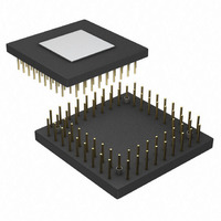
ADSP-2101BG-100 Analog Devices Inc, ADSP-2101BG-100 Datasheet - Page 12

ADSP-2101BG-100
Manufacturer Part Number
ADSP-2101BG-100
Description
Digital Signal Processor(DSP) IC
Manufacturer
Analog Devices Inc
Series
ADSP-21xxr
Type
Fixed Pointr
Datasheet
1.ADSP-2115BPZ-100.pdf
(64 pages)
Specifications of ADSP-2101BG-100
Rohs Status
RoHS non-compliant
Interface
Synchronous Serial Port (SSP)
Clock Rate
25MHz
Non-volatile Memory
External
On-chip Ram
6kB
Voltage - I/o
5.00V
Voltage - Core
5.00V
Operating Temperature
-40°C ~ 85°C
Mounting Type
Surface Mount
Package / Case
68-PGA
Package
68CPGA
Numeric And Arithmetic Format
Fixed-Point
Maximum Speed
25 MHz
Ram Size
3 KB
Device Million Instructions Per Second
25 MIPS
Lead Free Status / RoHS Status
Available stocks
Company
Part Number
Manufacturer
Quantity
Price
Company:
Part Number:
ADSP-2101BG-100
Manufacturer:
MICROCHIP
Quantity:
2 000
1K for ADSP-2101
ADSP-21xx
Data Memory Interface
The data memory address bus (DMA) is 14 bits wide. The
bidirectional external data bus is 24 bits wide, with the upper 16
bits used for data memory data (DMD) transfers.
The data memory select (DMS) signal indicates access to data
memory and can be used as a chip select signal. The write (WR)
signal indicates a write operation and can be used as a write
strobe. The read (RD) signal indicates a read operation and can
be used as a read strobe or output enable signal.
The ADSP-21xx processors support memory-mapped I/O, with
the peripherals memory-mapped into the data memory address
space and accessed by the processor in the same manner as data
memory.
Data Memory Map
ADSP-2101/ADSP-2103/ADSP-2111
For the ADSP-2101, ADSP-2103, and ADSP-2111, on-chip
data memory RAM resides in the 1K words beginning at
address 0x3800, as shown in Figure 10. Data memory locations
from 0x3C00 to the end of data memory at 0x3FFF are
reserved. Control and status registers for the system, timer,
wait-state configuration, and serial port operations are located in
this region of memory.
ADSP-2105/ADSP-2115
For the ADSP-2105 and ADSP-2115, on-chip data memory
RAM resides in the 512 words beginning at address 0x3800,
also shown in Figure 10. Data memory locations from 0x3A00
to the end of data memory at 0x3FFF are reserved. Control and
status registers for the system, timer, wait-state configuration,
and serial port operations are located in this region of memory.
ADSP-2103
ADSP-2111
Figure 10. Data Memory Map (All Processors)
CONTROL REGISTERS
512 for ADSP-2105
MEMORY-MAPPED
10K EXTERNAL
& RESERVED
1K EXTERNAL
1K EXTERNAL
1K EXTERNAL
1K EXTERNAL
DWAIT0
DWAIT1
DWAIT2
DWAIT3
DWAIT4
ADSP-2115
ADSP-216x
0x0000
0x3400
0x3A00
0x3C00
0x0400
0x0800
0x3000
0x3800
0x3FFF
EXTERNAL
INTERNAL
RAM
RAM
–12–
All Processors
The remaining 14K of data memory is located off-chip. This
external data memory is divided into five zones, each associated
with its own wait-state generator. This allows slower peripherals
to be memory-mapped into data memory for which wait states
are specified. By mapping peripherals into different zones, you
can accommodate peripherals with different wait-state require-
ments. All zones default to seven wait states after RESET.
Boot Memory Interface
On the ADSP-2101, ADSP-2103, and ADSP-2111, boot
memory is an external 64K by 8 space, divided into eight
separate 8K by 8 pages. On the ADSP-2105 and ADSP-2115,
boot memory is a 32K by 8 space, divided into eight separate
4K by 8 pages. The 8-bit bytes are automatically packed into
24-bit instruction words by each processor, for loading into on-
chip program memory.
Three bits in the processors’ System Control Register select
which page is loaded by the boot memory interface. Another bit
in the System Control Register allows the forcing of a boot
loading sequence under software control. Boot loading from
Page 0 after RESET is initiated automatically if MMAP = 0.
The boot memory interface can generate zero to seven wait
states; it defaults to three wait states after RESET. This allows
the ADSP-21xx to boot from a single low cost EPROM such as
a 27C256. Program memory is booted one byte at a time and
converted to 24-bit program memory words.
The BMS and RD signals are used to select and to strobe the
boot memory interface. Only 8-bit data is read over the data
bus, on pins D8-D15. To accommodate up to eight pages of
boot memory, the two MSBs of the data bus are used in the
boot memory interface as the two MSBs of the boot memory
address: D23, D22, and A13 supply the boot page number.
The ADSP-2100 Family Assembler and Linker allow the
creation of programs and data structures requiring multiple boot
pages during execution.
The BR signal is recognized during the booting sequence. The
bus is granted after loading the current byte is completed. BR
during booting may be used to implement booting under control
of a host processor.
Bus Interface
The ADSP-21xx processors can relinquish control of their data
and address buses to an external device. When the external
device requires control of the buses, it asserts the bus request
signal (BR). If the ADSP-21xx is not performing an external
memory access, it responds to the active BR input in the next
cycle by:
•
•
•
If the Go mode is set, however, the ADSP-21xx will not halt
program execution until it encounters an instruction that
requires an external memory access.
Three-stating the data and address buses and the PMS,
Asserting the bus grant (BG) signal,
and halting program execution.
DMS, BMS, RD, WR output drivers,
REV. B


