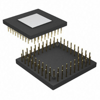
ADSP-2101BG-100 Analog Devices Inc, ADSP-2101BG-100 Datasheet - Page 20

ADSP-2101BG-100
Manufacturer Part Number
ADSP-2101BG-100
Description
Digital Signal Processor(DSP) IC
Manufacturer
Analog Devices Inc
Series
ADSP-21xxr
Type
Fixed Pointr
Datasheet
1.ADSP-2115BPZ-100.pdf
(64 pages)
Specifications of ADSP-2101BG-100
Rohs Status
RoHS non-compliant
Interface
Synchronous Serial Port (SSP)
Clock Rate
25MHz
Non-volatile Memory
External
On-chip Ram
6kB
Voltage - I/o
5.00V
Voltage - Core
5.00V
Operating Temperature
-40°C ~ 85°C
Mounting Type
Surface Mount
Package / Case
68-PGA
Package
68CPGA
Numeric And Arithmetic Format
Fixed-Point
Maximum Speed
25 MHz
Ram Size
3 KB
Device Million Instructions Per Second
25 MIPS
Lead Free Status / RoHS Status
Available stocks
Company
Part Number
Manufacturer
Quantity
Price
Company:
Part Number:
ADSP-2101BG-100
Manufacturer:
MICROCHIP
Quantity:
2 000
ADSP-21xx
SPECIFICATIONS (ADSP-2101/2105/2115/2161/2163)
TEST CONDITIONS
Figure 14 shows voltage reference levels for ac measurements.
Figure 14. Voltage Reference Levels for AC Measurements
(Except Output Enable/Disable)
Output Disable Time
Output pins are considered to be disabled when they have
stopped driving and started a transition from the measured
output high or low voltage to a high impedance state. The
output disable time (t
t
interval from when a reference signal reaches a high or low
voltage level to when the output voltages have changed by 0.5 V
from the measured output high or low voltage.
DECAY
, as shown in Figure 15. The time t
OUTPUT
INPUT
DIS
) is the difference of t
V
V
OH
OL
(MEASURED)
(MEASURED)
REFERENCE
SIGNAL
Figure 16. Equivalent Device Loading for AC Measurements
(Except Output Enable/Disable)
OUTPUT
OUTPUT
t
DECAY
MEASURED
1.5V
PIN
2.0V
0.8V
3.0V
1.5V
0.0V
OUTPUT STOPS
TO
t
MEASURED
t
DIS
MEASURED
DRIVING
Figure 15. Output Enable/Disable
50pF
is the
V
V
OH
OL
and
(MEASURED) – 0.5V
(MEASURED) +0.5V
–20–
I
I
OL
OH
The decay time, t
C
approximated by the following equation:
from which
is calculated. If multiple pins (such as the data bus) are dis-
abled, the measurement value is that of the last pin to stop
driving.
Output Enable Time
Output pins are considered to be enabled when they have made
a transition from a high-impedance state to when they start
driving. The output enable time (t
when a reference signal reaches a high or low voltage level to
when the output has reached a specified high or low trip point,
as shown in Figure 15. If multiple pins (such as the data bus)
are enabled, the measurement value is that of the first pin to
start driving.
L
HIGH-IMPEDANCE STATE.
TEST CONDITIONS CAUSE
THIS VOLTAGE LEVEL TO BE
APPROXIMATELY 1.5V.
, and the current load, i
OUTPUT STARTS
+1.5V
1.0V
2.0V
DRIVING
t
ENA
DECAY
t
DIS
t
DECAY
, is dependent on the capacitative load,
= t
L
MEASURED
, on the output pin. It can be
V
V
OH
OL
C
(MEASURED)
(MEASURED)
L
E NA
i
– t
0.5 V
L
) is the interval from
DECAY
REV. B


