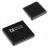
ADSP-2105BP-80 Analog Devices Inc, ADSP-2105BP-80 Datasheet - Page 32

ADSP-2105BP-80
Manufacturer Part Number
ADSP-2105BP-80
Description
IC,DSP,16-BIT,CMOS,LDCC,68PIN,PLASTIC
Manufacturer
Analog Devices Inc
Series
ADSP-21xxr
Type
Fixed Pointr
Datasheet
1.ADSP-2115BPZ-100.pdf
(64 pages)
Specifications of ADSP-2105BP-80
Rohs Status
RoHS non-compliant
Interface
Synchronous Serial Port (SSP)
Clock Rate
20MHz
Non-volatile Memory
External
On-chip Ram
3kB
Voltage - I/o
5.00V
Voltage - Core
5.00V
Operating Temperature
-40°C ~ 85°C
Mounting Type
Surface Mount
Package / Case
68-PLCC
Package
68PLCC
Numeric And Arithmetic Format
Fixed-Point
Maximum Speed
20 MHz
Ram Size
1.5 KB
Device Million Instructions Per Second
20 MIPS
Lead Free Status / RoHS Status
Available stocks
Company
Part Number
Manufacturer
Quantity
Price
Company:
Part Number:
ADSP-2105BP-80
Manufacturer:
TI
Quantity:
2 560
Company:
Part Number:
ADSP-2105BP-80
Manufacturer:
AD
Quantity:
42
Company:
Part Number:
ADSP-2105BP-80
Manufacturer:
AD
Quantity:
5 510
Company:
Part Number:
ADSP-2105BP-80
Manufacturer:
Analog Devices Inc
Quantity:
10 000
ADSP-21xx
TIMING PARAMETERS (ADSP-2101/2105/2111/2115/2161/2163)
BUS REQUEST/GRANT
Parameter
Timing Requirement:
t
t
Switching Characteristic:
t
t
t
t
NOTES
1
2
Section 10.2.4, “Bus Request/Grant,” on page 212 of the ADSP-2100 Family User’s Manual (1st Edition, 1993) states that “When BR is recognized, the processor
responds immediately by asserting BG during the same cycle.” This is incorrect for the current versions of all ADSP-21xx processors: BG is asserted in the cycle after
BR is recognized. No external synchronization circuit is needed when BR is generated as an asynchronous signal.
If BR meets the t
For 25 MHz only the minimum frequency dependency formula for t
BH
BS
SD
SDB
SE
SEC
a pulse width greater than 10 ns.
BR Hold after CLKOUT High
BR Setup before CLKOUT Low
CLKOUT High to DMS,
PMS, BMS, RD, WR Disable
DMS, PMS, BMS, RD, WR
Disable to BG Low
BG High to DMS, PMS,
BMS, RD, WR Enable
DMS, PMS, BMS, RD, WR
Enable to CLKOUT High
BS
and t
BH
setup/hold requirements, it will be recognized in the current processor cycle; otherwise it is recognized in the following cycle. BR requires
PMS, DMS
BMS, RD
CLKOUT
CLKOUT
WR
BG
BR
1
1
13 MHz
Min Max Min Max
24.2
39.2
0
0
9.2
39.2
t
SD
t
BH
13.824 MHz 16.67 MHz 20 MHz
23.1
38.1
0
0
8.1
Figure 31. Bus Request/Grant
t
BS
t
SDB
SEC
38.1
= (0.25t
–32–
Min Max Min Max Min Max Min
20
35
0
0
5
CK
– 8.5).
35
17.5
32.5
0
0
2.5
32.5
25 MHz
15
30
0
0
1.5
t
SE
2
t
SEC
30
Frequency
Dependency
0.25t
0.25t
0
0
0.25t
CK
CK
CK
+ 5
+ 20
– 10
2
Max
0.25t
CK
+ 20 ns
REV. B
Unit
ns
ns
ns
ns
ns


