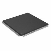
ADSP-21065LCSZ-240 Analog Devices Inc, ADSP-21065LCSZ-240 Datasheet - Page 36

ADSP-21065LCSZ-240
Manufacturer Part Number
ADSP-21065LCSZ-240
Description
ADSP-21065L 60 Mhz
Manufacturer
Analog Devices Inc
Series
SHARC®r
Type
Fixed/Floating Pointr
Datasheet
1.ADSP-21065LKSZ-240.pdf
(44 pages)
Specifications of ADSP-21065LCSZ-240
Interface
Host Interface, Serial Port
Clock Rate
60MHz
Non-volatile Memory
External
On-chip Ram
64kB
Voltage - I/o
3.30V
Voltage - Core
3.30V
Operating Temperature
-40°C ~ 100°C
Mounting Type
Surface Mount
Package / Case
208-MQFP, 208-PQFP
Device Core Size
32b
Architecture
Enhanced Harvard
Format
Floating Point
Clock Freq (max)
60MHz
Mips
60
Device Input Clock Speed
60MHz
Ram Size
68KB
Operating Supply Voltage (typ)
3.3V
Operating Supply Voltage (min)
3.13V
Operating Supply Voltage (max)
3.6V
Operating Temp Range
-40C to 100C
Operating Temperature Classification
Industrial
Mounting
Surface Mount
Pin Count
208
Package Type
MQFP
Lead Free Status / RoHS Status
Lead free / RoHS Compliant
Lead Free Status / RoHS Status
Lead free / RoHS Compliant
Other names
ADS-P21065LCSZ240
ADS-P21065LCSZ240
ADS-P21065LCSZ240
Available stocks
Company
Part Number
Manufacturer
Quantity
Price
Company:
Part Number:
ADSP-21065LCSZ-240
Manufacturer:
AD
Quantity:
310
Company:
Part Number:
ADSP-21065LCSZ-240
Manufacturer:
Analog Devices Inc
Quantity:
10 000
ADSP-21065L
OUTPUT DRIVE CURRENT
TEST CONDITIONS
Output Disable Time
Output pins are considered to be disabled when they stop driv-
ing, go into a high impedance state, and start to decay from
their output high or low voltage. The time for the voltage on the
bus to decay by DV is dependent on the capacitive load, C
the load current, I
the following equation:
The output disable time t
and t
interval from when the reference signal switches to when the
output voltage decays DV from the measured output high or
output low voltage. t
I
Output Enable Time
Output pins are considered to be enabled when they have made
a transition from a high impedance state to when they start
driving. The output enable time t
reference signal reaches a high or low voltage level to when the
output has reached a specified high or low trip point, as shown
in the Output Enable/Disable diagram. If multiple pins (such as
the data bus) are enabled, the measurement value is that of the
first pin to start driving.
L
, and with DV equal to 0.5 V.
DECAY
–100
–120
–20
–40
–60
–80
20
80
60
40
0
as shown in Figure 26. The time t
0
Figure 24. Typical Drive Currents
3.1V, +100 C
3.1V, +85 C
0.50
3.3V, +25 C
3.6V, –40 C
L
. This decay time can be approximated by
DECAY
t
DECAY
1.00
DIS
V
SOURCE VOLTAGE – V
OL
3.1V, +100 C
is calculated with test loads C
is the difference between t
1.50
=
C
ENA
L
3.3V, +25 C
2.00
I
¥ D
L
is the interval from when a
V
OH
V
2.50
3.1V, +85 C
3.6V, –40 C
MEASURED
3.00
3.50
MEASURED
is the
L
L
and
and
–36–
Example System Hold Time Calculation
To determine the data output hold time in a particular system,
first calculate t
to be the difference between the ADSP-21065L’s output voltage
and the input threshold for the device requiring the hold time. A
typical DV will be 0.4 V. C
data line), and I
data line). The hold time will be t
disable time (i.e., t
REFERENCE
Figure 26. Equivalent Device Loading for AC Measure-
ments (Includes All Fixtures)
Figure 27. Voltage Reference Levels for AC Measure-
ments (Except Output Enable/Disable)
V
V
OH (MEASURED)
OL (MEASURED)
OUTPUT
SIGNAL
INPUT OR
OUTPUT
t
OUTPUT
DIS
DECAY
OUTPUT STOPS
L
PIN
DRIVING
TO
is the total leakage or three-state current (per
Figure 25. Output Enable
DATRWH
1.5V
using the equation given above. Choose DV
50pF
t
MEASURED
V
V
OH (MEASURED)
OL (MEASURED)
t
DECAY
L
for the write cycle).
is the total bus capacitance (per
HIGH-IMPEDANCE STATE.
TEST CONDITIONS CAUSE
THIS VOLTAGE TO BE
APPROXIMATELY 1.5V
DECAY
+ V
I
– V
I
OH
OL
plus the minimum
OUTPUT STARTS
t
ENA
1.0V
2.0V
DRIVING
1.5V
+1.5V
V
V
OH (MEASURED)
OL (MEASURED)
REV. C


