ADSP-21262SBBC-150 Analog Devices Inc, ADSP-21262SBBC-150 Datasheet
ADSP-21262SBBC-150
Specifications of ADSP-21262SBBC-150
Available stocks


Related parts for ADSP-21262SBBC-150


ADSP-21262SBBC-150 Summary of contents
Page 1
... I channels of audio when all six serial ports (SPORTs) are enabled or six full duplex TDM streams 128 channels per frame At 200 MHz (5 ns) core instruction rate, the ADSP-21262 operates at 1200 MFLOPS peak/800 MFLOPS sustained ® port, six serial ...
Page 2
... DMA controller supports: 22 zero-overhead DMA channels for transfers between the ADSP-21262 internal memory and serial ports (12), the input data port (IDP) (eight), the SPI-compatible port (one), and the parallel port (one) 32-bit background DMA transfers at core clock speed, in ...
Page 3
... TABLE OF CONTENTS General Description ................................................. 4 ADSP-21262 Family Core Architecture ...................... 4 ADSP-21262 Memory and I/O Interface Features ......... 6 Target Board JTAG Emulator Connector .................... 8 Development Tools ............................................... 9 Evaluation Kit ..................................................... 10 Designing an Emulator-Compatible DSP Board (Target) ........................................... 10 Additional Information ......................................... 10 Pin Function Descriptions ........................................ 11 Address Data Pins as Flags ..................................... 14 Core Instruction Rate to CLKIN Ratio Modes ............. 14 Address Data Modes ...
Page 4
... ADSP-21266, ADSP-2136x, ADSP-2116x, and the first gen- eration ADSP-2106x SHARC DSPs. The ADSP-21262 shares 30 ns architectural features with the ADSP-2126x, ADSP-2136x, and 53.3 ns ADSP-2116x SIMD SHARC family of DSPs, as detailed in the following sections SIMD Computational Engine The ADSP-21262 contains two computational processing ele- ments that operate as a single-instruction multiple-data (SIMD) engine ...
Page 5
... Data Address Generators with Zero-Overhead Hardware Circular Buffer Support The ADSP-21262’s two data address generators (DAGs) are used for indirect addressing and implementing circular data buffers in hardware. Circular buffers allow efficient program- ming of delay lines and other data structures required in digital signal processing, and are commonly used in digital filters and Rev ...
Page 6
... IDP (input data port), parallel data acquisition port (PDAP), or the parallel port. Twenty-two channels of DMA are available on the ADSP-21262—one for the SPI, 12 via the serial ports, eight via the input data port, and one via the processor’s parallel port ...
Page 7
... Serial port clocks and frame syncs can be internally or externally generated. Serial Peripheral (Compatible) Interface Serial peripheral interface is an industry-standard synchronous 2 S channels serial link, enabling the ADSP-21262 SPI-compatible port to communicate with other SPI-compatible devices. SPI is an Rev Page August 2005 ADSP-21262 ADDRESS 0x0020 0000 ...
Page 8
... Timers The ADSP-21262 has a total of four timers: a core timer able to generate periodic software interrupts, and three general-pur- pose timers that can generate periodic interrupts and be independently set to operate in one of three modes: • ...
Page 9
... C/C++ runtime library that includes DSP and mathematical functions. A key point for these tools is C/C++ code efficiency. The compiler has been developed for efficient translation of C/C++ code to DSP assembly. The ADSP-21262 SHARC DSP has architectural features that improve the efficiency of compiled C/C++ code. ...
Page 10
... EZ-KIT Lite is a registered trademark of Analog Devices, Inc. ADDITIONAL INFORMATION ®† evaluation plat- This data sheet provides a general overview of the ADSP-21262 architecture and functionality. For detailed information on the ADSP-2126x family core architecture and instruction set, refer to the ADSP-2126x DSP Core Manual and the ADSP-21160 SHARC DSP Instruction Set Reference ...
Page 11
... P = power supply synchronous, (A/D) = active drive, (O/D) = open drain, and T = three-state. Function Parallel Port Address/Data. The ADSP-21262 parallel port and its corresponding DMA unit output addresses and data for peripherals on these multiplexed pins. The multiplex state is determined by the ALE pin. The parallel port can operate in either 8-bit or 16-bit mode. Each AD pin has a 22.5 kΩ ...
Page 12
... ADSP-21262 SPI interaction, any of the master ADSP-21262’s flag pins can be used to drive the SPIDS signal on the ADSP-21262 SPI slave device. SPI Master Out Slave In. If the ADSP-21262 is configured as a master, the MOSI pin becomes a data transmit (output) pin, transmitting output data. If the ADSP-21262 is configured as a slave, the MOSI pin becomes a data receive (input) pin, receiving input data ...
Page 13
... Three-state is a three-state driver, with pull-up disabled. Function Local Clock In. Used in conjunction with XTAL. CLKIN is the ADSP-21262 clock input. It configures the ADSP-21262 to use either its internal clock generator or an external clock source. Connecting the necessary components to CLKIN and XTAL enables the internal clock generator ...
Page 14
... ADSP-21262 ADDRESS DATA PINS AS FLAGS To use these pins as flags (FLAG15–0) set (=1) Bit 20 of the SYSCTL register and disable the parallel port. Table 3. AD15–0 to FLAG Pin Mapping AD Pin Flag Pin AD0 FLAG8 AD1 FLAG9 AD2 FLAG10 AD3 FLAG11 AD4 FLAG12 ...
Page 15
... ADSP-21262 SPECIFICATIONS RECOMMENDED OPERATING CONDITIONS 1 Parameter V Internal (Core) Supply Voltage DDINT A Analog (PLL) Supply Voltage VDD V External (I/O) Supply Voltage DDEXT V High Level Input Voltage IH V Low Level Input Voltage IL V High Level Input Voltage IH_CLKIN V Low Level Input Voltage @ V IL_CLKIN ...
Page 16
... ESD (electrostatic discharge) sensitive device. Electrostatic charges as high as 4000 V readily accumulate on the human body and test equipment and can discharge without detection. Although the ADSP-21262 features proprietary ESD protection circuitry, permanent damage may occur on devices subjected to high energy electrostatic discharges. Therefore, proper ESD precautions are recommended to avoid performance degradation or loss of functionality ...
Page 17
... TIMING SPECIFICATIONS The ADSP-21262’s internal clock (a multiple of CLKIN) pro- vides the clock signal for timing internal memory, processor core, serial ports, and parallel port (as required for read/write strobes in asynchronous access mode). During reset, program the ratio between the DSP’s internal clock frequency and exter- nal (CLKIN) clock frequency with the CLKCFG1– ...
Page 18
... ADSP-21262 Power-Up Sequencing The timing requirements for DSP startup are given in and Figure 6. Table 9. Power-Up Sequencing (DSP Startup) Parameter Timing Requirements t RESET Low Before V RSTVDD Before V IVDDEVDD DDINT t CLKIN Valid After V CLKVDD t CLKIN Valid Before RESET Deasserted CLKRST t PLL Control Setup Before RESET Deasserted ...
Page 19
... CKH Figure 7. Clock Input Clock Signals The ADSP-21262 can use an external clock or a crystal. See CLKIN pin description. The programmer can configure the ADSP-21262 to use its internal clock generator by connecting the necessary components to CLKIN and XTAL. the component connections used for a crystal operating in fun- damental mode ...
Page 20
... ADSP-21262 Reset See Table 11 and Figure 9. Table 11. Reset Parameter Timing Requirements t RESET Pulse Width Low WRST t RESET Setup Before CLKIN Low SRST Applies after the power-up sequence is complete. At power-up, the processor’s internal phase-locked loop requires no more than 100 µs while RESET is low, assuming 1 stable VDD and CLKIN (not including start-up time of external clock oscillator) ...
Page 21
... PWI DAI_P20–1 (TIMER) Figure 12 applies to Min 2 t – 1 CCLK t PWMO Figure 12. Timer PWM_OUT Timing Figure 13 applies to Min 2 t CCLK t PWI Figure 13. Timer Width Capture Timing Rev Page August 2005 ADSP-21262 Max Unit 31 2(2 – CCLK Max Unit 31 2(2 – CCLK ...
Page 22
... ADSP-21262 DAI Pin-to-Pin Direct Routing See Table 16 and Figure 14 for direct pin connections only (for example DAI_PB01_I to DAI_PB02_O). Table 16. DAI Pin-to-Pin Routing Parameter Timing Requirement t Delay DAI Pin Input Valid to DAI Output Valid DPIO DAI_Pn DAI_Pm t DPIO Figure 14. DAI Pin-to-Pin Direct Routing Rev ...
Page 23
... All timing parameters and switching characteris- tics apply to external DAI pins (DAI_P07 – DAI_P20). t STRIG t HTRIG t DPCGIO t DTRIG Figure 15. Precision Clock Generator (Direct Pin Routing) Rev Page August 2005 ADSP-21262 Min Max 2.5 10 2.5 + 2.5 × 2.5 × t PCGOW PCGOW ...
Page 24
... ADSP-21262 Flags The timing specifications in Table 18 and FLAG3–0 and DAI_P20–1 pins, the parallel port, and the serial peripheral interface. See Table 2 on Page 11 tion on flag use. Table 18. Flags Parameter Timing Requirement t FLAG3–0 IN Pulse Width FIPW Switching Characteristic t FLAG3–0 OUT Pulse Width FOPW DAI_P20– ...
Page 25
... Memory Read—Parallel Port The specifications in Table 19, Table 20, Figure 18 are for asynchronous interfacing to memories (and memory-mapped peripherals) when the ADSP-21262 is access- ing external memory space. Table 19. 8-Bit Memory Read Cycle Parameter Timing Requirements t Address/Data7–0 Setup Before RD High DRS t Address/Data7–0 Hold After RD High ...
Page 26
... ADSP-21262 Table 20. 16-Bit Memory Read Cycle Parameter Timing Requirements t Address/Data15–0 Setup Before RD high DRS t Address/Data15–0 Hold After RD high DRH Switching Characteristics t ALE Pulse Width ALEW t ALE Deasserted to Read/Write Asserted ALERW t Address/Data15–0 Setup Before ALE Deasserted ADAS t Address/Data15–0 Hold After ALE Deaserted ...
Page 27
... Memory Write—Parallel Port Use the specifications in Table 21, Table Figure 20 for asynchronous interfacing to memories (and memory-mapped peripherals) when the ADSP-21262 is access- ing external memory space. Table 21. 8-Bit Memory Write Cycle Parameter Switching Characteristics t ALE Pulse Width ALEW t ALE Deasserted to Read/Write Asserted ...
Page 28
... ADSP-21262 Table 22. 16-Bit Memory Write Cycle Parameter Switching Characteristics t ALE Pulse Width ALEW t ALE Deasserted to Read/Write Asserted ALERW t Address/Data 15–0 Setup Before ALE Deasserted ADAS t Address/Data15–0 Hold After ALE Deasserted ADAH t WR Pulse Width ALE Deasserted to Address/Data15–0 in High Z ALEHZ t Address/Data15– ...
Page 29
... Serial port signals (SCLK, FS, DxA,/DxB) are routed to the DAI_P20–1 pins using the SRU. Therefore, the timing specifica- tions provided below are valid at the DAI_P20–1 pins. Table 23, Table 24, must be confirmed Rev Page August 2005 ADSP-21262 Min Max Unit 2.5 ns 2.5 ns 2 Min Max Unit ...
Page 30
... ADSP-21262 Table 25. Serial Ports—Enable and Three-State Parameter Switching Characteristics t Data Enable from External Transmit SCLK DDTEN t Data Disable from External Transmit SCLK DDTTE t Data Enable from Internal Transmit SCLK DDTIN 1 Referenced to drive edge. Table 26. Serial Ports—External Late Frame Sync ...
Page 31
... DAI_P20–1 (SCLK HFSI SFSI DAI_P20–1 (FS) DAI_P20–1 (DATA CHANNEL A/B) t DDTEN t DDTIN Figure 22. Serial Ports Rev Page August 2005 ADSP-21262 DATA RECEIVE—EXTERNAL CLOCK DRIVE EDGE SAMPLE EDGE t SCLKW t DFSE t t SFSE HOFSE t SDRE DATA TRANSMIT—EXTERNAL CLOCK DRIVE EDGE ...
Page 32
... ADSP-21262 Input Data Port (IDP) The timing requirements for the IDP are given in Figure 23. IDP Signals (SCLK, FS, SDATA) are routed to the DAI_P20–1 pins using the SRU. Therefore, the timing specifica- tions provided below are valid at the DAI_P20–1 pins. Table 27. Input Data Port (IDP) ...
Page 33
... The timing requirements for the PDAP are provided in and Figure 24. PDAP is the parallel mode operation of Channel 0 of the IDP. For details on the operation of the IDP, see the IDP chapter of the ADSP-2126x Peripherals Manual. Table 28. Parallel Data Acquisition Port (PDAP) Parameter Timing Requirements t ...
Page 34
... ADSP-21262 SPI Protocol—Master Table 29. SPI Protocol—Master Parameter Timing Requirements t Data Input Valid to SPICLK Edge (Data Input Setup Time) SSPIDM t SPICLK Last Sampling Edge to Data Input Not Valid HSPIDM Switching Characteristics t Serial Clock Cycle SPICLKM t Serial Clock High Period SPICHM ...
Page 35
... SPICLK Edge to Data Out Not Valid (Data Out Hold Time) HDSPIDS t SPIDS Assertion to Data Out Valid (CPHASE = 0) DSOV Min 4 × × × × × × × × t Rev Page August 2005 ADSP-21262 Max Unit ns CCLK – CCLK – CCLK + 1 ns CCLK + 1 ns CCLK ns CCLK ...
Page 36
... ADSP-21262 SPIDS (INPUT SPICLK ( (INPUT SPICLK ( (INPUT MISO (OUTPUT) t CPHASE = MOSI MSB VALID (INPUT MISO MSB (OUTPUT) CPHASE = 0 MOSI MSB VALID (INPUT) JTAG Test Access Port and Emulation See Table 31 and Figure 27. Table 31. JTAG Test Access Port and Emulation Parameter Timing Requirements ...
Page 37
... TCK TCK t STAP TMS TDI t DTDO TDO t SSYS SYSTEM INPUTS t DSYS SYSTEM OUTPUTS Figure 27. JTAG Test Access Port and Emulation Rev Page August 2005 t HTAP t HSYS ADSP-21262 ...
Page 38
... ADSP-21262 OUTPUT DRIVE CURRENTS Figure 28 shows typical I-V characteristics for the output driv- ers of the ADSP-21262. The curves represent the current drive capability of the output drivers as a function of output voltage 3.11V, 125°C 0 –10 3.11V, 125°C –20 – 3.47V, –45°C – ...
Page 39
... LOAD CAPACITANCE (pF) Figure 33. Typical Output Delay or Hold vs. Load Capacitance (at Ambient Temperature) ENVIRONMENTAL CONDITIONS The ADSP-21262 processor is rated for performance under T environmental conditions specified in the AMB Operating Conditions on Page 15. THERMAL CHARACTERISTICS Table 32 through Table 36 airflow measurements comply with JEDEC standards JESD51-2 and JESD51-6 and the junction-to- board measurement complies with JESD51-8 ...
Page 40
... ADSP-21262 Table 35. Thermal Characteristics for Industrial Grade 136-Ball BGA (no thermal vias in PCB) Parameter Condition θ Airflow = 0 m/s JA θ Airflow = 1 m/s JMA θ Airflow = 2 m/s JMA θ JC Ψ Airflow = 0 m/s JT Ψ Airflow = 1 m/s JMT Ψ Airflow = 2 m/s JMT Table 36. Thermal Characteristics for Industrial ...
Page 41
... BGA PIN CONFIGURATIONS Table 37 shows the ADSP-21262’s pin names and their default function after reset (in parentheses). Figure 34 on Page 43 shows the BGA package pin assignments. Table 37. 136-Ball BGA Pin Assignments BGA Pin Pin Name No. Pin Name CLKCFG0 A01 CLKCFG1 ...
Page 42
... ADSP-21262 Table 37. 136-Ball BGA Pin Assignments (Continued) BGA Pin Pin Name No. Pin Name AD5 J01 AD3 AD4 J02 V DDINT GND J04 GND GND J05 GND GND J06 GND GND J09 GND GND J10 GND GND J11 GND V J13 GND DDINT DAI_P16 (SD4B) ...
Page 43
... KEY V A GND DDINT VDD V A I/O SIGNALS DDEXT VSS * USE THE CENTER BLOCK OF GROUND PINS TO PROVIDE THERMAL PATHWAYS TO YOUR PRINTED CIRCUIT BOARD’S GROUND PLANE. Figure 34. 136-Ball BGA Pin Assignments (Bottom View, Summary) Rev Page August 2005 ADSP-21262 ...
Page 44
... ADSP-21262 144-LEAD LQFP PIN CONFIGURATIONS Table 38 shows the ADSP-21262’s pin names and their default function after reset (in parentheses). Table 38. 144-Lead LQFP Pin Assignments LQFP Pin Name Pin No. Pin Name DDINT DDINT CLKCFG0 2 GND CLKCFG1 3 RD BOOTCFG0 4 ALE BOOTCFG1 5 AD15 GND ...
Page 45
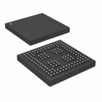
... PACKAGE DIMENSIONS The ADSP-21262 is available in a 136-ball BGA package and a 144-lead LQFP package shown in Figure 35 12.00 BSC SQ PIN A1 INDICATOR TOP VIEW 1.70 MAX 1. DIMENSIONS ARE IN MILIMETERS (MM). 2. THE ACTUAL POSITION OF THE BALL GRID IS WITHIN 0. ITS IDEAL POSITION RELATIVE TO THE PACKAGE EDGES. ...
Page 46
... ADSP-21262 ORDERING GUIDE Temperature 1 Model Range ADSP-21262SKBC-200 0°C to +70°C 2 ADSP-21262SKBCZ200 0°C to +70°C 2 ADSP-21262SKSTZ200 0°C to +70°C ADSP-21262SBBC-150 –40°C to +85°C 2 ADSP-21262SBBCZ150 –40°C to +85°C 1 Ranges shown represent ambient temperature. 2 Z=Pb-free part. Instruction On-Chip Rate SRAM ROM 200 MHz 2M bit 4M bit 1 ...
Page 47
... Rev Page August 2005 ADSP-21262 ...
Page 48
... ADSP-21262 © 2005 Analog Devices, Inc. All rights reserved. Trademarks and registered trademarks are the property of their respective owners. D04442-0-8/05(B) Rev Page August 2005 ...