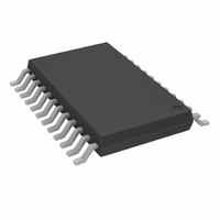
ADV7127KRU140 Analog Devices Inc, ADV7127KRU140 Datasheet - Page 8

ADV7127KRU140
Manufacturer Part Number
ADV7127KRU140
Description
IC,D/A CONVERTER,SINGLE,10-BIT,CMOS,TSSOP,24PIN
Manufacturer
Analog Devices Inc
Datasheet
1.ADV7127JRUZ240.pdf
(16 pages)
Specifications of ADV7127KRU140
Rohs Compliant
NO
Rohs Status
RoHS non-compliant
Settling Time
15ns
Number Of Bits
10
Data Interface
Parallel
Number Of Converters
1
Voltage Supply Source
Single Supply
Power Dissipation (max)
30mW
Operating Temperature
-40°C ~ 85°C
Mounting Type
Surface Mount
Package / Case
24-TSSOP
Number Of Channels
1
Resolution
10b
Interface Type
Parallel
Single Supply Voltage (typ)
3.3/5V
Dual Supply Voltage (typ)
Not RequiredV
Architecture
Segment
Power Supply Requirement
Single
Output Type
Current
Integral Nonlinearity Error
±1LSB
Single Supply Voltage (min)
3V
Single Supply Voltage (max)
5.25V
Dual Supply Voltage (min)
Not RequiredV
Dual Supply Voltage (max)
Not RequiredV
Operating Temp Range
-40C to 85C
Operating Temperature Classification
Industrial
Mounting
Surface Mount
Pin Count
24
Package Type
TSSOP
Lead Free Status / Rohs Status
Not Compliant
ADV7127
ABSOLUTE MAXIMUM RATINGS
V
Voltage on any Digital Pin . . . . . GND – 0.5 V to V
Ambient Operating Temperature (T
Storage Temperature (T
Junction Temperature (T
Lead Temperature (Soldering, 10 sec) . . . . . . . . . . . . +300 C
Vapor Phase Soldering (1 Minute) . . . . . . . . . . . . . . . . 220 C
I
NOTES
1
2
CAUTION
ESD (electrostatic discharge) sensitive device. Electrostatic charges as high as 4000 V readily
accumulate on the human body and test equipment and can discharge without detection.
Although the ADV7127 features proprietary ESD protection circuitry, permanent damage may
occur on devices subjected to high energy electrostatic discharges. Therefore, proper ESD
precautions are recommended to avoid performance degradation or loss of functionality.
Stresses above those listed under Absolute Maximum Ratings may cause perma-
Analog Output Short Circuit to any Power Supply or Common can be of an
nent damage to the device. This is a stress rating only; functional operation of the
device at these or any other conditions above those listed in the operational sections
of this specification is not implied. Exposure to absolute maximum rating condi-
tions for extended periods may affect device reliability.
indefinite duration.
OUT
AA
to GND . . . . . . . . . . . . . . . . . . . . . . . . . . . . . . . . . . +7 V
to GND
2
. . . . . . . . . . . . . . . . . . . . . . . . . . . . 0 V to V
NOTES
1
2
3
Package
R-28
RU-24
50 MHz and 140 MHz devices are specified for –40 C to +85 C operation; 240 MHz devices are specified for 0 C to +70 C.
SOIC Package.
TSSOP Package.
2
S
) . . . . . . . . . . . . . . –65 C to +150 C
J
) . . . . . . . . . . . . . . . . . . . . . +150 C
3
A
) . . . . . –40 C to +85 C
1
50 MHz
ADV7127KR50
ADV7127KRU50
AA
ORDERING GUIDE
+ 0.5 V
AA
–8–
Speed Options
140 MHz
ADV7127KR140
ADV7127KRU140
PDOWN
V
NC
D1
D2
D3
D4
D5
D6
D7
D8
D9
AA
24-Lead TSSOP
10
11
12
NC = NO CONNECT
1
2
3
4
5
6
7
8
9
1
(Not to Scale)
TOP VIEW
ADV7127
PIN CONFIGURATIONS
24
23
22
21
20
19
18
17
16
15
14
13
D0
PSAVE
R
V
COMP
I
I
V
GND
GND
CLOCK
NC
OUT
OUT
AA
SET
REF
240 MHz
ADV7127JR240
ADV7127JRU240
WARNING!
V
V
V
V
D0
D1
D2
D3
D4
D5
AA
D6
D7
D8
D9
AA
AA
AA
10
11
12
13
14
1
2
3
4
5
6
7
8
9
28-Lead SOIC
(Not to Scale)
ESD SENSITIVE DEVICE
ADV7127
TOP VIEW
28
27
26
25
24
23
22
21
20
19
18
17
16
15
REV. 0
V
V
PSAVE
R
V
COMP
V
I
V
GND
GND
CLOCK
V
V
OUT
AA
REF
AA
SET
AA
AA
AA
AA


