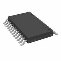
ADV7127KRU50 Analog Devices Inc, ADV7127KRU50 Datasheet - Page 9

ADV7127KRU50
Manufacturer Part Number
ADV7127KRU50
Description
Digital/Analog Converter IC Package/Case:24-TSSOP
Manufacturer
Analog Devices Inc
Datasheet
1.ADV7127JRUZ240.pdf
(16 pages)
Specifications of ADV7127KRU50
Leaded Process Compatible
No
A/d, D/a Features
CMOS, 240 MHz 10-Bit High Speed Video DAC
Peak Reflow Compatible (260 C)
No
Resolution
10-Bit
Settling Time
15nS
Rohs Status
RoHS non-compliant
Number Of Bits
10
Data Interface
Parallel
Number Of Converters
1
Voltage Supply Source
Single Supply
Power Dissipation (max)
30mW
Operating Temperature
-40°C ~ 85°C
Mounting Type
Surface Mount
Package / Case
24-TSSOP
Lead Free Status / RoHS Status
Contains lead / RoHS non-compliant
Available stocks
Company
Part Number
Manufacturer
Quantity
Price
Part Number:
ADV7127KRU50
Manufacturer:
ADI/亚德诺
Quantity:
20 000
Part Number:
ADV7127KRU50-REEL
Manufacturer:
ADI/亚德诺
Quantity:
20 000
Pin
Mnemonic
CLOCK
D0–D9
I
R
COMP
V
V
GND
I
PSAVE
PDOWN
TERMINOLOGY
Color Video (RGB)
This usually refers to the technique of combining the three
primary colors of red, green and blue to produce color pictures
within the usual spectrum. In RGB monitors, three DACs are
required, one for each color.
Gray Scale
The discrete levels of video signal between reference black and
reference white levels. A 10-bit DAC contains 1024 different
levels, while an 8-bit DAC contains 256.
Raster Scan
The most basic method of sweeping a CRT one line at a time to
generate and display images.
REV. 0
OUT
OUT
SET
REF
AA
Data Inputs (TTL Compatible). Data is latched on the rising edge of CLOCK. D0 is the least significant data bit.
Function
Clock Input (TTL Compatible). The rising edge of CLOCK latches the R0–R9, G0–G9, B0–B9, SYNC and
BLANK pixel and control inputs. It is typically the pixel clock rate of the video system. CLOCK should be driven
by a dedicated TTL buffer.
Unused data inputs should be connected to either the regular PCB power or ground plane.
Current Output. This high impedance current source is capable of directly driving a doubly terminated 75
coaxial cable.
Full-Scale Adjust Control. A resistor (R
full-scale video signal. Note that the IRE relationships are maintained, regardless of the full-scale output current.
The relationship between R
Compensation Pin. This is a compensation pin for the internal reference amplifier. A 0.1 F ceramic capacitor
must be connected between COMP and V
Voltage Reference Input. An external 1.23 V voltage reference must be connected to this pin. The use of an exter-
nal resistor divider network is not recommended. A 0.1 F decoupling ceramic capacitor should be connected
between V
Analog Power Supply (5 V
Ground. All GND pins must be connected.
Differential Current Output. Capable of directly driving a doubly terminated 75
put should be tied to ground.
Power Save Control Pin. The part is put into standby mode when PSAVE is low. The internal voltage reference
circuit is still active on the TSSOP in this case.
Power-Down Control Pin (24-Lead TSSOP Only). The ADV7127 completely powers down, including the voltage
reference circuit, when PDOWN is low.
REF
and V
AA
I
OUT
.
(mA) = 7968
SET
5%). All V
PIN FUNCTION DESCRIPTIONS
and the full-scale output current on I
SET
AA
V
AA
REF
) connected between this pin and GND controls the magnitude of the
pins on the ADV7127 must be connected.
.
(V)/R
–9–
Reference Black Level
The maximum negative polarity amplitude of the video signal.
Reference White Level
The maximum positive polarity amplitude of the video signal.
Video Signal
That portion of the composite video signal which varies in gray
scale levels between reference white and reference black. Also
referred to as the picture signal, this is the portion that may be
visually observed.
SET
( )
OUT
is given by:
load. If not required, this out-
ADV7127


