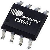
CS1501-FSZ Cirrus Logic Inc, CS1501-FSZ Datasheet

CS1501-FSZ
Specifications of CS1501-FSZ
Available stocks
Related parts for CS1501-FSZ
CS1501-FSZ Summary of contents
Page 1
... The CS1501 actively manages the power factor correction while achieving high efficiency over a wide load range. The CS1501 adaptively controls the input AC current so that phase with the AC mains voltage and its waveform mimics the input voltage waveform. The PFC controller executes ...
Page 2
... Figure 1. CS1501 Block Diagram the PFC active-switching behavior and efficiency. The auxiliary voltage is normalized using an external attenuator and is connected to the ZCD pin, providing the CS1501 a mechanism to detect the valley/zero crossings. The ZCD comparator looks for the zero crossing on the auxiliary winding and switches when the auxiliary voltage is below zero ...
Page 3
... CS ZCD 8-lead S OIC Figure 2. CS1501 Pin Assignments Link Voltage Sense — A current proportional to the output link voltage of the PFC is input into this pin. The current is measured with an ADC. Standby — A voltage below 0.8V puts the IC into a non-operating, low-power state. The input has an internal 600k pull-up resistor to the V Rectifier Voltage Sense — ...
Page 4
CHARACTERISTICS AND SPECIFICATIONS 3.1 Electrical Characteristics Typical characteristics conditions 25° 13V, GND = All voltages are measured with respect to GND. Unless otherwise specified, all current are positive when flowing into the ...
Page 5
... For test purposes, load capacitance ( VDD GND DS927PP6 Condition Symbol gate drive turns off I gate drive turns 1nF and is connected as shown in the following diagram. L +15V Buffer -15V 1nF CS1501 Min Typ Max - 31.6 BP(lower) - 39.6 BP(upper) T 134 147 159 SD(Hy 0 OUT S 2 Unit ...
Page 6
... Electrostatic Discharge Capability All Pins ESD Notes: 4. The CS1501 has an internal shunt regulator that limits the voltage on the V is defined in the VDD Supply Voltage 5. Long term operation at the maximum junction temperature will result in reduced product life. Derate internal power dissipation at the rate of 50mW/ °C for variation over temperature. ...
Page 7
... Figure 4. Supply Current (I 11 10.5 10 9.5 9 8 120 -60 Figure 6. Turn-on & Turn-off Threshold vs. Temp - Temperature ( Figure 7. Reference Current (I ) Drift vs. Temp ref f = 70kHz SW(max) Operating Start- 100 o Temperature ( Turn On Turn Off - Temperature ( C) 100 150 o C) CS1501 150 ) vs. Temp 140 7 ...
Page 8
Source Sink -60 -40 - Gate Resistor ( Figure 8. Gate Resistance (R 8 106% 104% 102 100 100 ...
Page 9
... Figure 11 illustrates how the frequency varies over one half cycle of the line voltage in steady-state operation. When power is first applied to the CS1501, it examines the line voltage and adapts its operating frequency to the line voltage as shown in Figure 11. The operating frequency is varied from the peak to the trough of the AC input ...
Page 10
... L > AC(rms) voltage of 400V. link . The magnitude of the I IFB IFB ref V link IFB CS1501 15k 24k IFB 1 Figure 17. IFB Input Pin Model , gives the B [Eq.3] , the link B 265 , is link current IFB current is then ) of 129A. I ref ADC DS927PP6 ...
Page 11
... Figure 19. ZCD Input Pin Model The objective of zero-voltage switching is to initiate each MOSFET switching cycle when its drain-source voltage is at the lowest possible voltage potential, thus reducing switching DS927PP6 losses. CS1501 uses an auxiliary winding on the PFC boost inductor to implement zero-voltage switching. – DD [Eq.4] ...
Page 12
... sustained overload repeated cycle of overload events BP(th) = BP(lower) IAC is detected for greater than 112 mS, the CS1501 shuts down for 2.5 seconds, then attempts to restart. Overvoltage Protection ) value. The IC ref – Equation 8 is used to calculate the ...
Page 13
... Standby (STBY) Function , fails (open or short to The standby (STBY) pin provides a means by which an external signal can cause the CS1501 to enter a non-operating, low-power state. The STBY input is intended to be driven by an open-collector/open-drain device. Internal to the pin, there is a pull-up resistor connected to the V shown in Figure 22 ...
Page 14
Summary of Equations Eq. # Equation Output Power 1 min Output Power w/ recommended values 2 P 90Vrms = o Boost Inductor 3 ...
Page 15
... SEATING PLANE e DIM 7. ORDERING INFORMATION Part # CS1501-FSZ 8. ENVIRONMENTAL, MANUFACTURING, & HANDLING INFORMATION Model Number CS1501-FSZ a. MSL (Moisture Sensitivity Level) as specified by IPC/JEDEC J-STD-020. b. Stored at 30°C, 60% relative humidity. DS927PP6 INCHES MIN MAX 0.053 0.069 0.004 0.010 0.013 0.020 0.007 0.010 ...
Page 16
REVISION HISTORY Revision Date PP1 NOV 2010 PP2 DEC 2010 PP3 JAN 2011 PP4 APR 2011 PP5 MAY 2011 PP6 JUN 2011 Contacting Cirrus Logic Support For all product questions and inquiries contact a Cirrus Logic Sales Representative. To ...


