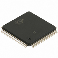
CY7C09099V-12AXC Cypress Semiconductor Corp, CY7C09099V-12AXC Datasheet

CY7C09099V-12AXC
Specifications of CY7C09099V-12AXC
Available stocks
Related parts for CY7C09099V-12AXC
CY7C09099V-12AXC Summary of contents
Page 1
... True Dual-Ported memory cells which enable simultaneous ■ access of the same memory location 6 Flow-Through and Pipelined devices ■ 32K x 8/9 organizations (CY7C09079V/179V) ■ 64K x 8/9 organizations (CY7C09089V/189V) ■ 128K x 8/9 organizations (CY7C09099V/199V) ■ 3 Modes ■ Flow-Through ■ Pipelined ■ Burst ■ ...
Page 2
... The internal write pulse width is independent of the LOW-to-HIGH transition of the clock signal. The internal write pulse is self-timed to enable the shortest possible cycle times. Pin Configurations Figure 1. 100-Pin TQFP (Top View) - CY7C09099V (128K x 8), CY7C09089V (64K x 8),CY7C09079V (32K x 8) 100 99 98 ...
Page 3
Pin Configurations (continued Figure 2. 100-Pin TQFP (Top View0 - CY7C09199V (128K x 9), CY7C09189V (64K x 9),CY7C09179V (32K x 9) 100 A7L 3 A8L 4 A9L 5 A10L 6 A11L 7 A12L ...
Page 4
Selection Guide CY7C09079V/89V/99V Description CY7C09179V/89V/99V-6 f (MHz) 100 MAX2 (Pipelined) Max. Access Time 6.5 (ns) (Clock to Data, Pipelined) Typical Operating 175 Current I (mA) CC Typical Standby 25 Current for I SB1 (mA) (Both Ports TTL Level) 10 μA ...
Page 5
... IN C Output Capacitance OUT Notes 10. The Voltage on any input or I/O pin cannot exceed the power pin during power-up. 11. Industrial parts are available in CY7C09099V and CY7C09199V only. 12. CE and CE are internal signals. To select either the left or right port, both Document #: 38-06043 Rev. *C Static Discharge Voltage............................................ > ...
Page 6
R1 = 590Ω OUTPUT 435Ω (a) Normal Load (Load 1) Figure 4. AC Test Loads (Applicable to -6 and -7 only 50Ω 50Ω 0 OUTPUT 1.4V ...
Page 7
Switching Characteristics Over the Operating Range Parameter Description f f Flow-Through MAX1 Max f f Pipelined MAX2 Max t Clock Cycle Time - Flow-Through CYC1 t Clock Cycle Time - Pipelined CYC2 t Clock HIGH Time - Flow-Through CH1 t ...
Page 8
Switching Waveforms (continued) Figure 6. Read Cycle for Flow-Through Output (FT/PIPE = CH1 CLK R ADDRESS t CD1 DATA ...
Page 9
Switching Waveforms (continued) Figure 7. Read Cycle for Pipelined Operation (FT/PIPE = V t CYC2 t CH2 CLK R ADDRESS Latency ...
Page 10
Switching Waveforms (continued) Figure 9. Left Port Write to Flow-Through Right Port Read CLK R ADDRESS MATCH VALID DATA INL t CCS CLK R t ...
Page 11
Switching Waveforms (continued) Figure 10. Pipelined Read-to-Write-to-Read ( CYC2 t t CH2 CL2 CLK R ADDRESS DATA IN ...
Page 12
Switching Waveforms (continued) Figure 11. Pipelined Read-to-Write-to-Read (OE Controlled) t CYC2 t t CH2 CL2 CLK R ADDRESS DATA IN DATA ...
Page 13
Switching Waveforms (continued) Figure 12. Flow-Through Read-to-Write-to-Read ( CYC1 t t CH1 CL1 CLK R ADDRESS DATA IN ...
Page 14
Switching Waveforms (continued) Figure 14. Pipelined Read with Address Counter Advance t CYC2 t t CH2 CL2 CLK ADDRESS SAD HAD ADS CNTEN t t SCN HCN DATA OUT Q Q x-1 ...
Page 15
Switching Waveforms (continued) Figure 16. Write with Address Counter Advance (Flow-Through or Pipelined Outputs) t CYC2 t t CH2 CL2 CLK ADDRESS n INTERNAL A n ADDRESS t t SAD HAD ADS CNTEN t t ...
Page 16
Switching Waveforms (continued) Figure 17. Counter Reset (Pipelined Outputs) t CYC2 t t CH2 CL2 CLK ADDRESS INTERNAL A X ADDRESS SAD HAD ADS t t SCN HCN CNTEN t t SRST HRST CNTRST t ...
Page 17
Table 1. Read/Write and Enable Operation Inputs OE CLK Table 2. Address Counter Control Operation Previous Address CLK ADS CNTEN Address ...
Page 18
... CY7C09089V-12AXI 128K x8 3.3V Synchronous Dual-Port SRAM Speed (ns) Ordering Code [1] 6.5 CY7C09099V-6AC CY7C09099V-6AXC [1] 7.5 CY7C09099V-7AC CY7C09099V-7AI CY7C09099V-7AXI 9 CY7C09099V-9AC CY7C09099V-9AI 12 CY7C09099V-12AC CY7C09099V-12AXC 32K x9 3.3V Synchronous Dual-Port SRAM Speed (ns) Ordering Code [1] 6.5 CY7C09179V-6AC CY7C09179V-6AXC [1] 7.5 CY7C09179V-7AC 9 CY7C09179V-9C 12 CY7C09179V-12AC CY7C09179V-12AXC Document #: 38-06043 Rev. *C Package Name ...
Page 19
Synchronous Dual-Port SRAM Speed (ns) Ordering Code [1] 6.5 CY7C09189V-6AC CY7C09189V-6AXC [1] 7.5 CY7C09189V-7AC 9 CY7C09189V-9AC 12 CY7C09189V-12AC CY7C09189V-12AXC 128K x9 3.3V Synchronous Dual-Port SRAM Speed (ns) Ordering Code [1] 6.5 CY7C09199V-6AC CY7C09199V-6AXC [1] 7.5 CY7C09199V-7AC CY7C09199V-7AXC ...
Page 20
Package Diagram Figure 18. 100-Pin Thin Plastic Quad Flat Pack (TQFP) A100 (51-85048) Document #: 38-06043 Rev. *C CY7C09079V/89V/99V CY7C09179V/89V/99V 51-85048-*B Page [+] Feedback ...
Page 21
... Change from Spec number: 38-00667 to 38-06043 Power up requirements added to Operating Conditions Information Added Pb-Free Logo Added Pb-Free Part Ordering Information: CY7C09089V-6AXC, CY7C09089V-12AXC, CY7C09099V-6AXC, CY7C09099V-7AI, CY7C09099V-7AXI, CY7C09099V-12AXC, CY7C09179V-6AXC, CY7C09179V-12AXC, CY7C09189V-6AXC, CY7C09189V-12AXC, CY7C09199V-6AXC, CY7C09199V-7AXC, CY7C09199V-9AXC, CY7C09199V-9AXI, CY7C09199V-12AXC Added CY7C09089V-12AXI part in the Ordering information table PSoC Solutions psoc ...


