CY7C1061AV33-10BAXIT Cypress Semiconductor Corp, CY7C1061AV33-10BAXIT Datasheet
CY7C1061AV33-10BAXIT
Specifications of CY7C1061AV33-10BAXIT
Available stocks


Related parts for CY7C1061AV33-10BAXIT


CY7C1061AV33-10BAXIT Summary of contents
Page 1
... Cypress Semiconductor Corporation Document #: 38-05256 Rev. *K 16-Mbit (1 M × 16) Static RAM Functional Description The CY7C1061AV33 is a high performance CMOS Static RAM organized as 1,048,576 words by 16 bits. To write to the device, enable the chip (CE while forcing the Write Enable (WE) input LOW. If Byte Low ...
Page 2
... Read Cycle No. 1 (Address Transition Controlled) ...... 6 Read Cycle No. 2 (OE Controlled) .............................. 6 Write Cycle No. 1 (CE1 or CE2 Controlled) ................ 7 Write Cycle No. 2 (WE Controlled, OE LOW) ............. 7 Write Cycle No. 3 (BHE/BLE Controlled) .................... 8 Document #: 38-05256 Rev. *K CY7C1061AV33 Truth Table ........................................................................ 8 Ordering Information ........................................................ 9 Ordering Code Definitions ........................................... 9 Package Diagrams .......................................................... 10 Acronyms ........................................................................ 12 Document Conventions ................................................. 12 Units of Measure ...
Page 3
... NC pins are not connected on the die. 2. DNU (Do Not Use) pins have to be left floating or tied to VSS to ensure proper operation. Document #: 38-05256 Rev. *K –10 10 Commercial 275 Industrial 275 Commercial/Industrial I I I CY7C1061AV33 Unit 54-pin TSOP II (Top View) I/O I I/O I I/O I I/O I ...
Page 4
... V CC [ components of the test environment. ALL INPUT PULSES 90% 90% 10% 10% Fall time: > 1 V/ns (c) to the data retention (V DD CY7C1061AV33 [3] ............................. –0 0 Ambient V CC Temperature 0 C to +70 C 3.3 V 0.3 V –40 C to +85 C –10 Min Max 2.4 – – ...
Page 5
... Read/Write operation is started. power , t are specified with a load capacitance (b) of LZBE LOW (CE HIGH) and WE LOW. Chip enables must be active and WE and byte enables must 1 2 and t HZWE CY7C1061AV33 –10 Unit Min Max 1 – – ns – 10 ...
Page 6
... WE is HIGH for Read cycle. 14. Address valid prior to or coincident with CE transition LOW and CE 1 Document #: 38-05256 Rev. *K DATA RETENTION MODE 3 > [12, 13 OHA DBE t DOE DATA VALID 50% . CE2 = transition HIGH. 2 CY7C1061AV33 3 DATA VALID HZCE t HZBE t HZOE HIGH IMPEDANCE Page [+] Feedback ...
Page 7
... HIGH simultaneously with WE going HIGH, the output remains in a high impedance state. 1 17. During this period, the IOs are in output state and input signals should not be applied. Document #: 38-05256 Rev. *K [15, 16 SCE PWE VALID DATA [15, 16 SCE PWE t SD VALID DATA . IH CY7C1061AV33 LZWE Page [+] Feedback ...
Page 8
... High Z Read Lower Bits Only High Z Data Out Read Upper Bits Only Data In Data In Write All Bits Data In High Z Write Lower Bits Only High Z Data In Write Upper Bits Only High Z High Z Selected, Outputs Disabled CY7C1061AV33 Mode Power Standby ( Standby ( Active ( Active (I ...
Page 9
... Ordering Information The following table lists the CY7C1061AV33 key package features and ordering codes. The table contains only the parts that are currently available. If you do not see what you are looking for, contact your local sales representative. For more information, visit the Cypress website at www ...
Page 10
... Package Diagrams Figure 1. 54-pin TSOP II (22.4 × 11.84 × 1.0 mm), 51-85160 Document #: 38-05256 Rev. *K CY7C1061AV33 51-85160 *A Page [+] Feedback ...
Page 11
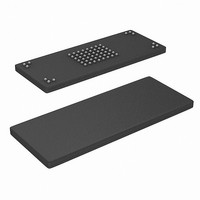
... Package Diagrams (continued) Figure 2. 60-ball FBGA (8 × 20 × 1.2 mm), 51-85162 Document #: 38-05256 Rev. *K CY7C1061AV33 51-85162 *E Page [+] Feedback ...
Page 12
... I/O input/output OE output enable SRAM static random access memory TSOP thin small-outline package TTL transistor-transistor logic WE Write Enable Document #: 38-05256 Rev. *K CY7C1061AV33 Document Conventions Units of Measure Symbol Unit of Measure ns nano seconds V Volts µA micro Amperes mA milli Amperes mm ...
Page 13
... Document History Page Document Title: CY7C1061AV33 16-Mbit (1 M × 16) Static RAM Document Number: 38-05256 Submission Revision ECN Date ** 113725 03/28/02 *A 117058 07/31/02 *B 117989 08/30/02 *C 120383 11/06/02 *D 124439 2/25/03 *E 492137 See ECN *F 508117 See ECN *G 877322 See ECN *H 2897049 03/22/10 *I 3109147 12/13/2010 ...
Page 14
... Cypress against all charges. Use may be limited by and subject to the applicable Cypress software license agreement. Document #: 38-05256 Rev. *K All products and company names mentioned in this document may be the trademarks of their respective holders. cypress.com/go/plc Revised April 11, 2011 CY7C1061AV33 PSoC Solutions psoc.cypress.com/solutions PSoC 1 | PSoC 3 ...