CY7C1069DV33-10BVXI Cypress Semiconductor Corp, CY7C1069DV33-10BVXI Datasheet
CY7C1069DV33-10BVXI
Specifications of CY7C1069DV33-10BVXI
Available stocks


Related parts for CY7C1069DV33-10BVXI

CY7C1069DV33-10BVXI Summary of contents
Page 1
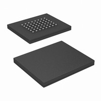
... LOW), the outputs are disabled (OE HIGH), or during a write features 2 2 operation (CE LOW The CY7C1069DV33 is available in a 54-pin TSOP II package with center power and ground (revolutionary) pinout, and a 48-Ball very fine pitch ball grid array (VFBGA) package. INPUT BUFFER ARRAY COLUMN DECODER • ...
Page 2
... Thermal Resistance ..........................................................5 AC Test Loads and Waveforms .......................................5 Capacitance .......................................................................5 AC Switching Characteristics ..........................................6 Data Retention Characteristics ........................................7 Data Retention Waveform ................................................7 Switching Waveforms .......................................................7 Document Number: 38-05478 Rev. *F CY7C1069DV33 Truth Table ........................................................................9 Ordering Information ........................................................9 Ordering Code Definitions ...........................................9 Package Diagrams ..........................................................10 Acronyms ........................................................................12 Document Conventions .................................................12 Units of Measure .......................................................12 Document History Page .................................................13 Sales, Solutions, and Legal Information ...
Page 3
... Maximum CMOS standby current Pin Configuration Figure 1. 54-Pin TSOP II (Top View Note 1. NC pins are not connected on the die. Document Number: 38-05478 Rev. *F [1] Figure 2. 48-Ball VFBGA (Top View CY7C1069DV33 –10 Unit 10 ns 175 [ I Page [+] Feedback ...
Page 4
... CE > < IL, V > < MAX Max > V – 0 < 0 > V – 0 < 0 CY7C1069DV33 Ambient V CC Temperature –40 C to +85 C 3.3 V 0.3 V –10 Unit Min Max 2.4 – V – 0 –0.3 0.8 V A –1 +1 A –1 +1 – 175 mA – ...
Page 5
... SRAM operation begins including reduction Document Number: 38-05478 Rev. *F Test Conditions = 25 MHz 3 Test Conditions [3] High-Z characteristics = 1 ALL INPUT PULSES 90% 90% 10% ( the data retention (V , 2.0V) voltage. DD CCDR CY7C1069DV33 TSOP II VFBGA Unit TSOP II VFBGA Unit C/W 24.18 28.37 C/W 5.40 5.79 R1 317 3.3 V OUTPUT R2 5 pF* 351 ...
Page 6
... LOW to High Z 2 [7] HIGH to power-up 2 [7] LOW to power-down 2 HIGH to write end 2 [6] [6] values until the first memory access is performed Test Loads and = V , and and t HZWE CY7C1069DV33 –10 Unit Min Max s 100 – 10 – ns – – ns – – – ns – 5 ...
Page 7
... V > CDR [12, 13] Figure 3. Read Cycle No OHA ACE t DOE t LZOE DATA VALID 50% > 50 s or stable at V > 50 CC(min.) CC(min transition HIGH. 2 CY7C1069DV33 Min Max Unit 2 – – < 0 – – 3 DATA VALID [13, 14] t HZOE t HZCE HIGH IMPEDANCE t PD 50% Page ...
Page 8
... shorthand combination of both CE and CE 1 16. Data IO is high impedance 17 goes HIGH simultaneously with WE going HIGH, the output remains in a high impedance state. Document Number: 38-05478 Rev SCE PWE SCE PWE t t HZWE SD combined active LOW. 2 CY7C1069DV33 [15, 16, 17 [15, 16, 17 LZWE Page [+] Feedback ...
Page 9
... Ordering Information Speed Ordering Code (ns) 10 CY7C1069DV33-10ZSXI CY7C1069DV33-10BVXI Ordering Code Definitions V33 - 10 XXX Document Number: 38-05478 Rev. *F I/O – I/O Mode 0 7 High Z Power-down High Z Power-down Data out Read all bits Data in Write all bits High Z Selected, outputs disabled Package Package Type ...
Page 10
... Package Diagrams Document Number: 38-05478 Rev. *F Figure 7. 54-pin TSOP Type II CY7C1069DV33 51-85160 *A Page [+] Feedback ...
Page 11
... Package Diagrams (continued) Document Number: 38-05478 Rev. *F Figure 8. 48-ball VFBGA ( mm) CY7C1069DV33 51-85178 *A Page [+] Feedback ...
Page 12
... TSOP thin small outline package TTL Transistor transistor logic Document Conventions Units of Measure Symbol Unit of Measure °C degrees Celsius A microamperes mA milliampere MHz megahertz ns nanoseconds pF picofarads V volts ohms W watts Document Number: 38-05478 Rev. *F CY7C1069DV33 Page [+] Feedback ...
Page 13
... Document History Page Document Title: CY7C1069DV33 16-Mbit (2 M × 8) Static RAM Document Number: 38-05478 Orig. of REV. ECN NO. Issue Date Change ** 201560 See ECN SWI *A 233748 See ECN RKF *B 469420 See ECN NXR *C 499604 See ECN NXR *D 1462585 See ECN VKN/AESA Converted from preliminary to final ...
Page 14
... Cypress against all charges. Use may be limited by and subject to the applicable Cypress software license agreement. Document Number: 38-05478 Rev. *F All products and company names mentioned in this document may be the trademarks of their respective holders. cypress.com/go/plc Revised January 19, 2011 CY7C1069DV33 PSoC Solutions psoc.cypress.com/solutions PSoC 1 | PSoC 3 ...