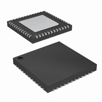
CYWUSB6935-48LTXC Cypress Semiconductor Corp, CYWUSB6935-48LTXC Datasheet - Page 13

CYWUSB6935-48LTXC
Manufacturer Part Number
CYWUSB6935-48LTXC
Description
CYWUSB6935-48LTXC
Manufacturer
Cypress Semiconductor Corp
Specifications of CYWUSB6935-48LTXC
Frequency
2.4GHz
Data Rate - Maximum
62.5kbps
Modulation Or Protocol
DSSS, GFSK
Applications
AMR, ISM, RKE
Power - Output
0dBm
Sensitivity
-95dBm
Voltage - Supply
2.7 V ~ 3.6 V
Current - Receiving
57.7mA
Current - Transmitting
69.1mA
Data Interface
PCB, Surface Mount
Antenna Connector
PCB, Surface Mount
Operating Temperature
0°C ~ 70°C
Package / Case
48-VQFN Exposed Pad, 48-HVQFN, 48-SQFN, 48-DHVQFN
Operating Temperature (min)
-40C
Operating Temperature (max)
85C
Operating Temperature Classification
Industrial
Product Depth (mm)
7mm
Product Length (mm)
7mm
Operating Supply Voltage (min)
2.7V
Operating Supply Voltage (typ)
3V
Operating Supply Voltage (max)
3.6V
Lead Free Status / RoHS Status
Lead free / RoHS Compliant
Memory Size
-
Lead Free Status / Rohs Status
Compliant
Available stocks
Company
Part Number
Manufacturer
Quantity
Price
Company:
Part Number:
CYWUSB6935-48LTXC
Manufacturer:
ST
Quantity:
1 200
Table 11. Receive SERDES Data A
Table 12. Receive SERDES Valid A
Table 13. Receive SERDES Data B
Table 14. Receive SERDES Valid B
Document #: 38-16008 Rev. *E
Bit
7:0 Valid
Bit
7:0 Data
Bit Name
7:0 Valid
Bit
7:0 Data
Name
Name
Name
7
7
7
7
Addr: 0x0A
Addr: 0x0B
Addr: 0x0C
Addr: 0x09
These bits indicate which of the bits in the Receive SERDES Data B register (Reg 0x0B) are valid. A “1” indicates that
the corresponding data bit is valid for Channel B.
If the Valid Data bit is set in the Receive Interrupt Status register (0x08) all eight bits in the Receive SERDES Data B
register (Reg 0x0B) are valid. Therefore, it is not necessary to read the Receive SERDES Valid B register (Reg 0x0C).
This register is read-only.
Received Data for Channel A. The over-the-air received order is bit 0 followed by bit 1, followed by bit 2, followed by
bit 3, followed by bit 4, followed by bit 5, followed by bit 6, followed by bit 7. This register is read-only.
These bits indicate which of the bits in the Receive SERDES Data A register (Reg 0x09) are valid. A “1” indicates that
the corresponding data bit is valid for Channel A.
If the Valid Data bit is set in the Receive Interrupt Status register (Reg 0x08) all eight bits in the Receive SERDES Data
A register (Reg 0x09) are valid. Therefore, it is not necessary to read the Receive SERDES Valid A register (Reg 0x0A).
This register is read-only.
Received Data for Channel B. The over-the-air received order is bit 0 followed by bit 1, followed by bit 2, followed by
bit 3, followed by bit 4, followed by bit 5, followed by bit 6, followed by bit 7. This register is read-only.
6
6
6
6
5
5
5
5
REG_RX_VALID_A
REG_RX_VALID_B
REG_RX_DATA_A
REG_RX_DATA_B
4
4
4
4
Valid
Valid
Data
Data
Description
Description
Description
Description
3
3
3
3
2
2
2
2
1
1
1
1
CYWUSB6935
Default: 0x00
Default: 0x00
Default: 0x00
Default: 0x00
Page 13 of 34
0
0
0
0
[+] Feedback


