CYWUSB6935-48LTXI Cypress Semiconductor Corp, CYWUSB6935-48LTXI Datasheet
CYWUSB6935-48LTXI
Specifications of CYWUSB6935-48LTXI


Related parts for CYWUSB6935-48LTXI


CYWUSB6935-48LTXI Summary of contents
Page 1
... The CYWUSB6935 transceiver is a single-chip 2.4 GHz DSSS Gaussian Frequency Shift Keying (GFSK) baseband modem radio that connects directly to a microcontroller via a simple serial peripheral interface. The CYWUSB6935 is offered in an industrial temperature range 48-pin QFN and a commercial temperature range 48-pin QFN. GFSK DSSS ...
Page 2
... Application Interfaces ...................................................... 4 SPI Interface ................................................................ 4 DIO Interface ............................................................... 6 Interrupts ..................................................................... 6 Application Examples ...................................................... 7 Register Descriptions ...................................................... 8 Absolute Maximum Ratings .......................................... 25 Document Number : 38-16008 Rev. *G CYWUSB6935 Operating Conditions ..................................................... 25 DC Characteristics (Over the Operating Range) ............ 25 AC Characteristics ......................................................... 26 Radio Parameters ..................................................... 28 Power Management Timing ...................................... 29 Typical Operating Characteristics ............................. 30 Ordering Information ...................................................... 32 Ordering Code Definition ........................................... 32 Package Diagram ...
Page 3
... Forty-nine spreading codes selected for optimal performance (Gold codes) are supported across 78 1-MHz channels yielding a theoretical spectral capacity of 3822 channels. The CYWUSB6935 supports a range meters or more. Document Number : 38-16008 Rev. *G CYWUSB6935 2.4 GHz Radio ...
Page 4
... The radio frequency (RF) circuitry has on-chip decoupling capac- itors. The CYWUSB6935 is powered from a 2.7-V to 3.6-V DC supply. The CYWUSB6935 can be shut down to a fully static state using the PD pin. Receive Signal Strength Indicator (RSSI) The RSSI register (Reg 0x22) returns the relative signal strength of the ON-channel signal power and can be used to: 1 ...
Page 5
... DIR INC ISO Document Number : 38-16008 Rev. *G [5:0] Address Figure 1. SPI Single Read Sequence Figure 2. SPI Burst Read Sequence Figure 3. SPI Single Write Sequence data from Figure 4. SPI Burst Write Sequence d ata fro from CYWUSB6935 Byte 1+N [7:0] Data Page [+] Feedback ...
Page 6
... The application MCU samples the DIO and DIOVAL on the rising edge of IRQ. Interrupts The CYWUSB6935 features three sets of interrupts: transmit, received, and a wake interrupt. These interrupts all share a single pin (IRQ), but can be independently enabled/disabled. In transmit mode, all receive interrupts are automatically disabled, and in receive mode all transmit interrupts are automatically disabled ...
Page 7
... Application Examples Figure 7 shows a block diagram example of a typical battery powered device using the CYWUSB6935 chip. Figure 8 shows an application example of a WirelessUSB LR alarm system where a single hub node is connected to an alarm panel. The hub node wirelessly receives information from multiple sensor nodes in order to control the alarm panel. ...
Page 8
... Register Descriptions Table 3 displays the list of registers inside the CYWUSB6935 that are addressable through the SPI interface. All registers are read and writable, except where noted. [1] Table 3. CYWUSB6935 Register Map Register Name Revision ID REG_ID Control REG_CONTROL Data Rate REG_DATA_RATE Configuration REG_CONFIG ...
Page 9
... This bit is reserved and should be written with a zero. 0 Reserved This bit is reserved and should be written with a zero. Document Number : 38-16008 Rev. *G REG_ID Description REG_CONTROL Bypass Internal Auto Internal Internal PA Syn Lock PA Enable Signal Disable Description CYWUSB6935 Default: 0x07 1 0 Product ID Default: 0x00 1 0 Reserved Reserved Page [+] Feedback ...
Page 10
... The following Reg 0x04, bits 2:0 values are not valid: • 001–Not Valid • 010–Not Valid • 011–Not Valid • 111–Not Valid Document Number : 38-16008 Rev. *G REG_DATA_RATE Code Width Description CYWUSB6935 Default: 0x00 1 0 Data Rate Sample Rate Page [+] Feedback ...
Page 11
... the EOF length, an EOF condition will occur at the first invalid bit after a valid reception. Document Number : 38-16008 Rev. *G REG_CONFIG 4 3 Reserved Description REG_SERDES_CTL 4 3 SERDES Enable Description CYWUSB6935 Default: 0x01 IRQ Pin Select Default: 0x03 EOF Length Page [+] Feedback ...
Page 12
... A Full A condition occurs when data is transferred from the Channel A Receiver into the Receive SERDES Data A register (Reg 0x09). This could occur when a complete byte is received or when an EOF event occurs whether or not a complete byte has been received. Document Number : 38-16008 Rev. *G REG_RX_INT_EN Full B Underflow A Overflow A Description CYWUSB6935 Default: 0x00 1 0 EOF A Full A Page [+] Feedback ...
Page 13
... TX Enable and RX Enable (Reg 0x03, bits 7:6). For example, the receive status will read 0 if the IC is not in receive mode. These registers are read-only. Document Number : 38-16008 Rev. *G [3] REG_RX_INT_STAT Full B Valid A Description CYWUSB6935 Default: 0x00 Flow Violation A EOF A Full A Page [+] Feedback ...
Page 14
... Therefore not necessary to read the Receive SERDES Valid B register (Reg 0x0C). This register is read-only. Document Number : 38-16008 Rev. *G REG_RX_DATA_A Data Description REG_RX_VALID_A Valid Description REG_RX_DATA_B Data Description REG_RX_VALID_B Valid Description CYWUSB6935 Default: 0x00 1 0 Default: 0x00 1 0 Default: 0x00 1 0 Default: 0x00 1 0 Page [+] Feedback ...
Page 15
... Empty interrupt disabled The Empty condition occurs when the Transmit SERDES Data register (Reg 0x0F) is loaded into the transmit buffer and it's safe to load the next byte Document Number : 38-16008 Rev. *G REG_TX_INT_EN Underflow Overflow Description CYWUSB6935 Default: 0x00 1 0 Done Empty Page [+] Feedback ...
Page 16
... TX Enable and RX Enable (Reg 0x03, bits 7:6). For example, the transmit status will read 0 if the IC is not in transmit mode. These registers are read-only. Document Number : 38-16008 Rev. *G [4] REG_TX_INT_STAT 4 3 Underflow Overflow Description CYWUSB6935 Default: 0x00 Done Empty Page [+] Feedback ...
Page 17
... LSB first. The SERDES will continue to send data until there are no more VALID bits in the shifter. For example, writing 0x0F to the Transmit SERDES Valid register (Reg 0x10) will send half a byte. Document Number : 38-16008 Rev. *G REG_TX_DATA 4 3 Data Description REG_TX_VALID 4 3 Valid Description REG_PN_CODE Address 0x17 Address 0x16 Address 0x13 Address 0x12 Description CYWUSB6935 Default: 0x00 Default: 0x00 Default: 0x1E8B6A3DE0E9B222 Address 0x15 ...
Page 18
... A wakeup event is triggered when the PD pin is deasserted and once the IC is ready to receive SPI communi- cations. Document Number : 38-16008 Rev. *G REG_THRESHOLD_L Threshold Low Description REG_THRESHOLD_H Threshold High Description REG_WAKE_EN Reserved Description CYWUSB6935 Default: 0x08 1 0 Default: 0x38 1 0 Default: 0x00 1 0 Wakeup Enable Page [+] Feedback ...
Page 19
... The application MCU must ensure that this register is modified before transmitting data over the air for the first time. Document Number : 38-16008 Rev. *G REG_WAKE_STAT Reserved Description REG_ANALOG_CTL Reserved Reserved PA Output Enable Description REG_CHANNEL Channel Description CYWUSB6935 Default: 0x01 1 0 Wakeup Status Default: 0x00 Invert Reset Default: 0x00 1 0 Page [+] Feedback ...
Page 20
... The RSSI will collect a single value each time the part is put into receive mode via Control register (Reg 0x03, bit 7=1). See Section for more details. Document Number : 38-16008 Rev. *G [6] REG_RSSI RSSI Description REG_PA Description REG_CRYSTAL_ADJ Crystal Adjust Description CYWUSB6935 Default: 0x00 1 0 Default: 0x00 Bias Table 1 for typical output power Default: 0x00 1 0 Page [+] Feedback ...
Page 21
... Manual Clock Overrides This register must be written with 0x41 after reset for correct operation Document Number : 38-16008 Rev. *G REG_VCO_CAL Reserved Description REG_PWR_CTL Reserved Description REG_CARRIER_DETECT Reserved Description REG_CLOCK_MANUAL Manual Clock Overrides Description CYWUSB6935 Default: 0x00 1 0 Default: 0x00 1 0 Default: 0x00 1 0 Default: 0x00 1 0 Page [+] Feedback ...
Page 22
... Manufacturing ID register (Reg 0x3C-0x3F). This register is read-only. Document Number : 38-16008 Rev. *G REG_CLOCK_ENABLE 4 3 Manual Clock Enables Description REG_SYN_LOCK_CNT 4 3 Count Description REG_MID Address 0x3E Address 0x3D Description CYWUSB6935 Default: 0x00 Default: 0x64 ...
Page 23
... Master-Output-Slave-Input Data. SPI data input pin. Hi-Z Master-Input-Slave-Output Data. SPI data output pin. N/A SPI Input Clock. SPI clock. N/A Slave Select Enable. SPI enable 2.7V to 3.6V Ground = Must be tied to Ground. N/A L Must be tied to Ground. CYWUSB6935 Description on page 4). on page 4). Page [+] Feedback ...
Page 24
... RFOUT E-PAD BOTTOM SIDE Document Number : 38-16008 Rev. *G Figure 9. CYWUSB6935 48 QFN – Top View CYWUSB6935 Top View CYWUSB6935 6 48 QFN CYWUSB6935 X13IN 34 PACTL X13OUT 25 SCK Page [+] Feedback ...
Page 25
... –2 2 < V < HIGH [13] to inputs through a series resistor limiting input current to 1 mA. This can’t be done during power down mode. to inputs through a series resistor limiting input current to 1 mA. CYWUSB6935 [9] [10] [12] Min Typ Max Unit 2.7 3.0 3.6 V – 0.1 V – ...
Page 26
... SCK must start low, otherwise the success of SPI transactions are not guaranteed. Document Number : 38-16008 Rev. *G Description Figure 10. SPI Timing Diagram fro SCK_LO SCK_H I (BURST READ) th every 9 SCK_HI data DAT_VAL . CC CYWUSB6935 Min Typ Max Unit 476 – – ns 238 – – ns 158 – – ns 158 – – – – ...
Page 27
... Figure 12. DIO Receive Timing Diagram Figure 13. DIO Transmit Timing Diagram _IR _IR Q _LO data X_D X_D IO VA L_S CYWUSB6935 Typ. Max. Unit – – µs – – µs 0 – – µs 0 – – µs – 8 – µs – 16 – ...
Page 28
... C = –67 dBm [21 –67 dBm C = –64 dBm Δ 5,10 MHz ± 2 ppm seven steps, monotonic PN Code Pattern 10101010 PN Code Pattern 11110000 100-kHz resolution bandwidth, –6 dBc CYWUSB6935 Min Typ Max Unit 2.400 – 2.483 GHz –3 ) –86 –95 – dBm –20 – ...
Page 29
... Figure 14. Power On Reset/Reset Timing Figure 15. Sleep / Wake Timing t WAKE t t WAKE_INT Figure 15 illustrates a wakeup event configured to trigger an IRQ pin event via the Wake Enable register CYWUSB6935 [27] Min Typ Max Unit – 2000 – µs 1 – – ...
Page 30
... BER Sensitivity vs Vcc @ -45°C -95.0 -95.5 -96.0 -96.5 -97.0 -97.5 -98 2.5 2.7 CYWUSB6935 BER Sensitivity vs Temp GUID: 0x0ECC7E75 3.3 3.7 2 100 Temperature (°C) - Tem perature (°C) LR06 0x0ECC7E75 LR07 0x17D34AAD LR14 0x0DD2E9F8 2.9 3.1 3.3 3.5 3 ...
Page 31
... Spec M in -0.8 Spec Typ -1 Temp Spec -1.2 -1.4 -1.6 -1 -60 -40 CYWUSB6935 BER Sensitivity vs Vcc @ 90°C LR06 0x0EC C7E75 LR07 0x17D34AAD LR14 0x0DD 2E9F8 2.9 3.1 3.3 3.5 3.7 Vcc Tx Ch40 Output Power LR18 0x17D34E2D 2.6 3.3 3.7 ...
Page 32
... JIG AND SCOPE Max Parameter R1 1071 R2 937 R 500 3.00 CC Ordering Information Part Number Radio CYWUSB6935-48LTXI Transceiver CYWUSB6935-48LTXC Transceiver Ordering Code Definition C/I CY 6935 48-LTX WUSB Document Number : 38-16008 Rev Test Load OUTPUT 5 pF OUTPUT INCLUDING JIG AND SCOPE Typical Unit ...
Page 33
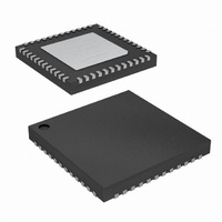
... Package Diagram Figure 17. 48-pin QFN 7 × 7 × 1.0 mm LT48C (Sawn) Document Number : 38-16008 Rev. *G CYWUSB6935 001-53698 *A Page [+] Feedback ...
Page 34
... Non return to zero PLL Phase locked loop QFN Quad flat no-leads RSSI Received signal strength indication RF Radio frequency Rx Receive Tx Transmit Document Number : 38-16008 Rev. *G CYWUSB6935 Document Conventions Table 42. Units of Measure Symbol Unit of Measure °C degree Celsius dB decibels dBc decibel relative to carrier dBm decibel-milliwatt Hz ...
Page 35
... Document History Page Document Title: CYWUSB6935 WirelessUSB Document Number: 38-16008 Orig. of Submission Revision ECN Change Date ** 207428 TGE 02/27/04 *A 275349 ZTK See ECN *B 291015 ZTK See ECN *C 335774 TGE See ECN *D 391311 TGE See ECN *E 2770967 DPT 09/29/09 *F 2897889 TGE 03/23/10 ...
Page 36
... Cypress against all charges. Use may be limited by and subject to the applicable Cypress software license agreement. Document Number : 38-16008 Rev. *G All products and company names mentioned in this document may be the trademarks of their respective holders. cypress.com/go/plc Revised October 05, 2010 CYWUSB6935 PSoC Solutions psoc.cypress.com/solutions PSoC 1 | PSoC 3 ...