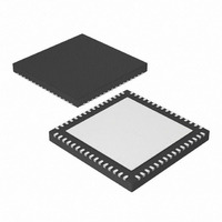
DSPIC33FJ128MC706AT-I/MR Microchip Technology, DSPIC33FJ128MC706AT-I/MR Datasheet - Page 264

DSPIC33FJ128MC706AT-I/MR
Manufacturer Part Number
DSPIC33FJ128MC706AT-I/MR
Description
16 Bit MCU/DSP 40MIPS 128KB FLASH 64 QFN 9x9x0.9mm T/R
Manufacturer
Microchip Technology
Series
dsPIC™ 33Fr
Datasheet
1.DSPIC33FJ64MC506A-IPT.pdf
(352 pages)
Specifications of DSPIC33FJ128MC706AT-I/MR
Core Processor
dsPIC
Core Size
16-Bit
Speed
40 MIPs
Connectivity
CAN, I²C, IrDA, LIN, SPI, UART/USART
Peripherals
Brown-out Detect/Reset, DMA, Motor Control PWM, QEI, POR, PWM, WDT
Number Of I /o
53
Program Memory Size
128KB (128K x 8)
Program Memory Type
FLASH
Ram Size
16K x 8
Voltage - Supply (vcc/vdd)
3 V ~ 3.6 V
Data Converters
A/D 16x10b/12b
Oscillator Type
Internal
Operating Temperature
-40°C ~ 85°C
Package / Case
64-VFQFN, Exposed Pad
Lead Free Status / RoHS Status
Lead free / RoHS Compliant
Eeprom Size
-
Lead Free Status / RoHS Status
Lead free / RoHS Compliant
- Current page: 264 of 352
- Download datasheet (3Mb)
dsPIC33FJXXXMCX06A/X08A/X10A
All instructions are a single word, except for certain
double-word instructions, which were made double-
word instructions so that all the required information is
available in these 48 bits. In the second word, the
8 MSbs are ‘0’s. If this second word is executed as an
instruction (by itself), it will execute as a NOP.
Most single-word instructions are executed in a single
instruction cycle, unless a conditional test is true, or the
program counter is changed as a result of the instruction.
In these cases, the execution takes two instruction cycles
with the additional instruction cycle(s) executed as a NOP.
Notable exceptions are the BRA (unconditional/computed
branch), indirect CALL/GOTO, all table reads and writes
TABLE 24-1:
DS70594B-page 264
#text
(text)
[text]
{ }
<n:m>
.b
.d
.S
.w
Acc
AWB
bit4
C, DC, N, OV, Z
Expr
f
lit1
lit4
lit5
lit8
lit10
lit14
lit16
lit23
None
OA, OB, SA, SB
PC
Slit10
Slit16
Slit6
Wb
Wd
Wdo
Wm,Wn
Field
SYMBOLS USED IN OPCODE DESCRIPTIONS
Means literal defined by “text”
Means “content of text”
Means “the location addressed by text”
Optional field or operation
Register bit field
Byte mode selection
Double-Word mode selection
Shadow register select
Word mode selection (default)
One of two accumulators {A, B}
Accumulator Write-Back Destination Address register {W13, [W13]+ = 2}
4-bit bit selection field (used in word addressed instructions) {0...15}
MCU Status bits: Carry, Digit Carry, Negative, Overflow, Sticky Zero
Absolute address, label or expression (resolved by the linker)
File register address {0x0000...0x1FFF}
1-bit unsigned literal {0,1}
4-bit unsigned literal {0...15}
5-bit unsigned literal {0...31}
8-bit unsigned literal {0...255}
10-bit unsigned literal {0...255} for Byte mode, {0:1023} for Word mode
14-bit unsigned literal {0...16384}
16-bit unsigned literal {0...65535}
23-bit unsigned literal {0...8388608}; LSb must be ‘0’
Field does not require an entry, may be blank
DSP Status bits: AccA Overflow, AccB Overflow, AccA Saturate, AccB Saturate
Program Counter
10-bit signed literal {-512...511}
16-bit signed literal {-32768...32767}
6-bit signed literal {-16...16}
Base W register {W0..W15}
Destination W register { Wd, [Wd], [Wd++], [Wd--], [++Wd], [--Wd] }
Destination W register
{ Wnd, [Wnd], [Wnd++], [Wnd--], [++Wnd], [--Wnd], [Wnd+Wb] }
Dividend, Divisor working register pair (direct addressing)
Preliminary
Moreover, double-word moves require two cycles. The
double-word instructions execute in two instruction
and RETURN/RETFIE instructions, which are single-
word instructions but take two or three cycles. Certain
instructions that involve skipping over the subsequent
instruction require either two or three cycles if the skip is
performed, depending on whether the instruction being
skipped is a single-word or two-word instruction.
cycles.
Note:
Description
For more details on the instruction set,
refer to the “dsPIC30F/33F Programmer’s
Reference Manual” (DS70157).
2009 Microchip Technology Inc.
Related parts for DSPIC33FJ128MC706AT-I/MR
Image
Part Number
Description
Manufacturer
Datasheet
Request
R

Part Number:
Description:
Manufacturer:
Microchip Technology Inc.
Datasheet:

Part Number:
Description:
Manufacturer:
Microchip Technology Inc.
Datasheet:

Part Number:
Description:
Manufacturer:
Microchip Technology Inc.
Datasheet:

Part Number:
Description:
Manufacturer:
Microchip Technology Inc.
Datasheet:

Part Number:
Description:
Manufacturer:
Microchip Technology Inc.
Datasheet:

Part Number:
Description:
Manufacturer:
Microchip Technology Inc.
Datasheet:

Part Number:
Description:
Manufacturer:
Microchip Technology Inc.
Datasheet:

Part Number:
Description:
Manufacturer:
Microchip Technology Inc.
Datasheet:


