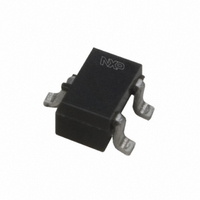
BAV199W,115 NXP Semiconductors, BAV199W,115 Datasheet

BAV199W,115
Specifications of BAV199W,115
934054800115
BAV199W T/R
BAV199W T/R
BAV199W,115
Related parts for BAV199W,115
BAV199W,115 Summary of contents
Page 1
DATA SHEET dbook, halfpage BAV199W Low-leakage double diode Product data sheet Supersedes data of 1998 Jan 09 DISCRETE SEMICONDUCTORS M3D102 1999 May 11 ...
Page 2
... NXP Semiconductors Low-leakage double diode FEATURES • Small plastic SMD package • Low leakage current: typ • Switching time: typ. 0.8 μs • Continuous reverse voltage: max • Repetitive peak reverse voltage: max • Repetitive peak forward current: max. 500 mA. ...
Page 3
... NXP Semiconductors Low-leakage double diode ELECTRICAL CHARACTERISTICS = 25 °C unless otherwise specified SYMBOL PARAMETER Per diode V forward voltage F I reverse current R C diode capacitance d t reverse recovery time rr THERMAL CHARACTERISTICS SYMBOL R thermal resistance from junction to soldering point th j-s 1999 May 11 CONDITIONS see Fig.3 ...
Page 4
... NXP Semiconductors Low-leakage double diode GRAPHICAL DATA 300 handbook, halfpage I F (mA) (1) 200 (2) 100 0 0 100 (1) Single diode loaded. (2) Double diodes loaded. Fig.2 Maximum permissible continuous forward current as a function of soldering point temperature; per diode handbook, full pagewidth I FSM ( − Based on square wave currents. ...
Page 5
... NXP Semiconductors Low-leakage double diode 2 10 handbook, halfpage I R (nA 100 (1) Maximum values. (2) Typical values. Fig.5 Reverse current as a function of junction temperature; per diode. handbook, full pagewidth D.U. Ω ( mA. R Input signal: reverse pulse rise time t Oscilloscope: rise time t = 0.35 ns. ...
Page 6
... NXP Semiconductors Low-leakage double diode PACKAGE OUTLINE Plastic surface mounted package; 3 leads DIMENSIONS (mm are the original dimensions UNIT max 1.1 0.4 0.25 mm 0.1 0.8 0.3 0.10 OUTLINE VERSION IEC SOT323 1999 May scale 2.2 1.35 2.2 1.3 0.65 1.8 1.15 2.0 ...
Page 7
... NXP Semiconductors. In case of any inconsistency or conflict between information in this document and such terms and conditions, the latter will prevail. ...
Page 8
... NXP Semiconductors Customer notification This data sheet was changed to reflect the new company name NXP Semiconductors. No changes were made to the content, except for the legal definitions and disclaimers. Contact information For additional information please visit: http://www.nxp.com For sales offices addresses send e-mail to: salesaddresses@nxp.com © ...


