BAS56,235 NXP Semiconductors, BAS56,235 Datasheet
BAS56,235
Specifications of BAS56,235
BAS56 /T3
BAS56 /T3


Related parts for BAS56,235


BAS56,235 Summary of contents
Page 1
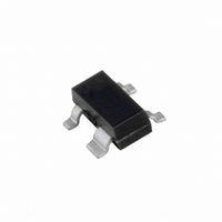
BAS56 High-speed double diode Rev. 3 — 29 June 2010 1. Product profile 1.1 General description Two high-speed switching diodes fabricated in planar technology, and encapsulated in a small SOT143B Surface-Mounted Device (SMD) plastic package. The diodes are not connected. ...
Page 2
... NXP Semiconductors 2. Pinning information Table 2. Pin Ordering information Table 3. Type number BAS56 4. Marking Table 4. Type number BAS56 [ made in Hong Kong * = p: made in Hong Kong * = t: made in Malaysia * = W: made in China BAS56 Product data sheet Pinning Description cathode (diode 1) cathode (diode 2) anode (diode 2) anode (diode 1) ...
Page 3
... NXP Semiconductors 5. Limiting values Table 5. In accordance with the Absolute Maximum Rating System (IEC 60134). Symbol V RRM FRM I FSM P tot stg [1] Series connection. [2] Device mounted on an FR4 PCB. [3] Single diode loaded. [4] Double diode loaded °C prior to surge. [ Thermal characteristics Table 6. Symbol ...
Page 4
... NXP Semiconductors 7. Characteristics Table 7. ° Symbol [1] T amb [2] Series connection. [3] When switched from I [4] When switched from I [5] When switched from I BAS56 Product data sheet Characteristics C unless otherwise specified. Parameter Conditions forward voltage I = 200 mA F reverse current diode capacitance MHz; V reverse recovery time forward recovery voltage = 25 ° ...
Page 5
... NXP Semiconductors 300 I F (mA) 200 100 ° Fig 1. Forward current as a function of forward voltage; typical values (μA) 10 (1) (2) 1 −1 10 − 100 ( maximum values R ( typical values R Fig 3. Reverse current as a function of junction temperature BAS56 Product data sheet mbh279 FSM ( − (V) F Fig 2. ...
Page 6
... NXP Semiconductors (1) Single diode loaded (2) Double diode loaded Fig 5. 8. Test information D.U. Ω × ( Fig 6. Reverse recovery time test circuit and waveforms I 450 Ω 1 kΩ Ω D.U.T. Input signal: pulse duration t Fig 7. Forward recovery voltage test circuit and waveforms ...
Page 7
... NXP Semiconductors 8.1 Quality information This product has been qualified in accordance with the Automotive Electronics Council (AEC) standard Q101 - Stress test qualification for discrete semiconductors, and is suitable for use in automotive applications. 9. Package outline Fig 8. 10. Packing information Table 8. The indicated -xxx are the last three digits of the 12NC ordering code. ...
Page 8
... NXP Semiconductors 11. Soldering 0.7 (3×) 0.7 Fig 9. 4.6 Fig 10. Wave soldering footprint BAS56 (SOT143B) BAS56 Product data sheet 3.25 0.6 (3×) 0.5 (3×) 1.9 0.6 (3×) 0.6 0.75 0.95 0.9 1 Reflow soldering footprint BAS56 (SOT143B) 4.45 2.2 2.575 1.2 All information provided in this document is subject to legal disclaimers. ...
Page 9
... Release date BAS56 v.3 20100629 • Modifications: The format of this data sheet has been redesigned to comply with the new identity guidelines of NXP Semiconductors. • Legal texts have been adapted to the new company name where appropriate. • Section 1.1 “General • Section 4 • ...
Page 10
... In no event shall NXP Semiconductors be liable for any indirect, incidental, punitive, special or consequential damages (including - without limitation - lost profits, lost savings, business interruption, costs related to the removal or ...
Page 11
... NXP Semiconductors Quick reference data — The Quick reference data is an extract of the product data given in the Limiting values and Characteristics sections of this document, and as such is not complete, exhaustive or legally binding. 14. Contact information For more information, please visit: For sales office addresses, please send an email to: ...
Page 12
... NXP Semiconductors 15. Contents 1 Product profile . . . . . . . . . . . . . . . . . . . . . . . . . . 1 1.1 General description . . . . . . . . . . . . . . . . . . . . . 1 1.2 Features and benefits . . . . . . . . . . . . . . . . . . . . 1 1.3 Applications . . . . . . . . . . . . . . . . . . . . . . . . . . . 1 1.4 Quick reference data . . . . . . . . . . . . . . . . . . . . 1 2 Pinning information . . . . . . . . . . . . . . . . . . . . . . 2 3 Ordering information . . . . . . . . . . . . . . . . . . . . . 2 4 Marking . . . . . . . . . . . . . . . . . . . . . . . . . . . . . . . . 2 5 Limiting values Thermal characteristics . . . . . . . . . . . . . . . . . . 3 7 Characteristics . . . . . . . . . . . . . . . . . . . . . . . . . . 4 8 Test information . . . . . . . . . . . . . . . . . . . . . . . . . 6 8.1 Quality information . . . . . . . . . . . . . . . . . . . . . . 7 9 Package outline . . . . . . . . . . . . . . . . . . . . . . . . . 7 10 Packing information ...