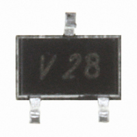
HBAT-540C-TR1G Avago Technologies US Inc., HBAT-540C-TR1G Datasheet - Page 6

HBAT-540C-TR1G
Manufacturer Part Number
HBAT-540C-TR1G
Description
DIODE SCHOTTKY 30V 430MA SOT-323
Manufacturer
Avago Technologies US Inc.
Datasheet
1.HBAT-5402-BLKG.pdf
(8 pages)
Specifications of HBAT-540C-TR1G
Voltage - Reverse Standoff (typ)
30V
Voltage - Breakdown
30V
Power (watts)
825mW
Polarization
Bidirectional
Mounting Type
Surface Mount
Package / Case
SC-70-3, SOT-323-3
Speed
Fast Recovery =< 500ns, > 200mA (Io)
Voltage - Dc Reverse (vr) (max)
30V
Current - Average Rectified (io) (per Diode)
430mA (DC)
Diode Configuration
1 Pair Series Connection
Capacitance Ct
3pF
Diode Case Style
SOT-323
Series Resistance @ If
2.4ohm
Peak Reflow Compatible (260 C)
Yes
Reel Quantity
3000
Leaded Process Compatible
Yes
Diode Type
RF Schottky
Breakdown Voltage
30V
Forward Voltage
800mV
Rohs Compliant
Yes
Lead Free Status / RoHS Status
Lead free / RoHS Compliant
Reverse Recovery Time (trr)
-
Current - Reverse Leakage @ Vr
-
Voltage - Forward (vf) (max) @ If
-
Lead Free Status / RoHS Status
Lead free / RoHS Compliant, Lead free / RoHS Compliant
Other names
516-1785-2
HBAT-540C-TR1G
HBAT-540C-TR1G
Available stocks
Company
Part Number
Manufacturer
Quantity
Price
Company:
Part Number:
HBAT-540C-TR1G
Manufacturer:
AVAGO
Quantity:
8 000
Part Number:
HBAT-540C-TR1G
Manufacturer:
AVAGO/安华高
Quantity:
20 000
Applications Information
Schottky Diode Fundamentals
The HBAT-540x series of clipping/clamping diodes
are Schottky devices. A Schottky device is a rectifying,
metal-semiconductor contact formed between a metal
and an n-doped or a p-doped semiconductor. When a
metal-semiconductor junction is formed, free electrons
fl ow across the junction from the semiconductor and fi ll
the free-energy states in the metal. This fl ow of electrons
creates a depletion or potential across the junction. The
diff erence in energy levels between semiconductor and
metal is called a Schottky barrier.
P-doped, Schottky-barrier diodes excel at applications
requiring ultra low turn-on voltage (such as zero-biased
RF detectors). But their very low, breakdown-voltage
and high series-resistance make them unsuitable for
the clipping and clamping applications involving high
forward currents and high reverse voltages. Therefore,
this discussion will focus entirely on n-doped Schottky
diodes.
Under a forward bias (metal connected to positive in an
n-doped Schottky), or forward voltage, V
electrons with enough thermal energy to cross the barrier
potential into the metal. Once the applied bias exceeds
the built-in potential of the junction, the forward current,
I
When the Schottky diode is reverse biased, the potential
barrier for electrons becomes large; hence, there is
a small probability that an electron will have suffi -
cient thermal energy to cross the junction. The reverse
leakage current will be in the nanoampere to microam-
pere range, depending upon the diode type, the reverse
voltage, and the temperature.
In contrast to a conventional p-n junction, current in
the Schottky diode is carried only by majority carriers.
Because no minority carrier charge storage eff ects are
present, Schottky diodes have carrier lifetimes of less
than 100 ps and are extremely fast switching semi-
conductors. Schottky diodes are used as rectifi ers at
frequencies of 50 GHz and higher.
Another signifi cant diff erence between Schottky and
p-n diodes is the forward voltage drop. Schottky diodes
have a threshold of typically 0.3 V in comparison to that
of 0.6 V in p-n junction diodes. See Figure 6.
6
F
, will increase rapidly as V
F
increases.
F
, there are many
CAPACITANCE
Figure 6.
Through the careful manipulation of the diameter of the
Schottky contact and the choice of metal deposited on
the n-doped silicon, the important characteristics of the
diode (junction capacitance, C
tance, R
V
270x series and HBAT-540x series of diodes are a case in
point.
Both diodes have similar barrier heights; and this
is indicated by corresponding values of saturation
current, I
layer thickness result in very diff erent values of junction
capacitance, C
parameters in Table 1.
Table 1. HBAT-540x and HSMS-270x SPICE Parameters.
At low values of I
two diodes are nearly identical. However, as current rises
above 10 mA, the lower series resistance of the HSMS-
270x allows for a much lower forward voltage. This gives
the HSMS-270x a much higher current handling capabil-
ity. The trade-off is a higher value of junction capacitance.
The forward voltage and current plots illustrate the diff er-
ences in these two Schottky diodes, as shown in Figure
7.
Parameter
BV
CJ0
EG
IBV
IS
N
RS
PB
PT
M
F
,) can be optimized for specifi c applications. The HSMS-
PN JUNCTION
BIAS VOLTAGE
–
S
P
; breakdown voltage, V
S
. Yet, diff erent contact diameters and epitaxial-
N
+
0.6V
J
CURRENT
and R
HBAT-540x
F
1.0E-7 A
10E-4 A
0.55 eV
3.0 pF
2.4 Ω
≤ 1 mA, the forward voltages of the
0.6 V
40 V
1.0
0.5
2
S
CAPACITANCE
. This is portrayed by their SPICE
SCHOTTKY JUNCTION
BIAS VOLTAGE
–
METAL N
BR
+
J
CURRENT
0.3V
; parasitic series resis-
; and forward voltage,
HSMS-270x
1.4E-7 A
10E-4 A
0.55 eV
0.65 Ω
6.7 pF
0.6 V
25 V
1.04
0.5
2


