TISP4145J1BJR-S Bourns Inc., TISP4145J1BJR-S Datasheet
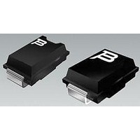
Sidacs 120V(DRM) 1KA(IPP)145V(BO)

TISP4145J1BJR-S

Manufacturer Part Number
TISP4145J1BJR-S
Description
Sidacs 120V(DRM) 1KA(IPP)145V(BO)
Manufacturer
Bourns Inc.
Datasheet

Specifications of TISP4145J1BJR-S

Breakover Current Ibo Max
100 A
Rated Repetitive Off-state Voltage Vdrm
120 V
Off-state Leakage Current @ Vdrm Idrm
0.005 mA
Mounting Style
SMD/SMT
Package / Case
DO-214AA
Lead Free Status / RoHS Status
Lead free / RoHS Compliant

Available stocks

Company
Part Number
Manufacturer
Quantity
Price
Part Number:
TISP4145J1BJR-S
Manufacturer:
BOURNS
Quantity:
240 000
*RoHS Directive 2002/95/EC Jan 27 2003 including Annex
Specifications are subject to change without notice.
Customers should verify actual device performance in their specific applications.
Ground Return Element of Y Configuration
-2x Current Capability of Y Upper Elements
-Available in a Wide Range of Voltages
-Enables Symmetrical and Asymmetrical Y Designs
-SMB (DO-214AA) Package
Ion-Implanted Breakdown Region
-Precise and Stable Voltage
-Low Voltage Overshoot Under Surge
The TISP4xxxJ1BJ is a symmetrical voltage-triggered bidirectional thyristor device which has been designed as the tail (ground return) element
of a Y circuit configured protector. As such, the TISP4xxxJ1BJ must be rated to conduct the sum of the TIP and RING currents. For example,
the normal GR-1089-CORE testing can impose 200 A, 10/1000 and 1000 A, 2/10 on the ground return element of the Y configuration. Using
the TISP4xxxJ1BJ together with two TISP4xxxH3BJ parts gives a 2x 100 A, 10/1000 Y protector circuit. For ITU-T applications, using the
TISP4xxxJ1BJ with a TISP3xxxT3BJ gives a coordinated Y protector with a 2x 120 A, 5/310 capability. Design tables are given in the
Applications Information section. These SMB package combinations are often more space efficient than single package Y protection
multi-chip integrations.
These devices allow signal voltages, without clipping, up to the maximum off-state voltage value, V
limited and will not exceed the breakover voltage, V
voltage on-state condition, which diverts the current from the overvoltage through the device. When the diverted current falls below the
holding current, I
SEPTEMBER 2001 - REVISED JANUARY 2007
Description
How to Order
TISP 4xxxJ1BJ
Device
............................................ UL Recognized Components
TISP4070J1
TISP4080J1
TISP4095J1
TISP4115J1
TISP4125J1
TISP4145J1
TISP4165J1
TISP4180J1
TISP4200J1
TISP4219J1
TISP4250J1
TISP4290J1
TISP4350J1
TISP4395J1
Device
H
, level the devices switches off and restores normal system operation.
B J (SMB/D O - 214AA J-Bend)
Package
V
100
120
135
145
155
180
190
220
275
320
DRM
58
65
75
90
V
V
115
125
145
165
180
200
219
250
290
350
395
(BO)
TISP4xxxJ1BJ Overvoltage Protector Series
70
80
95
V
(BO)
R (Embossed T ape Re eled)
, level. If sufficient current flows due to the overvoltage, the device switches into a low-
Carrier
BIDIRECTIONAL THYRISTOR OVERVOLTAGE PROTECTORS
Rated for International Surge Wave Shapes
SMB Package (Top View)
Device Symbol
Wave Shape
10/1000
10/160
10/700
10/560
2/10
8/20
TISP4xxxJ1BJR-S
Order As
MT1
TISP4070J1BJ THRU TISP4395J1BJ
TIA/EIA-IS-968 (FCC Part 68)
DRM
1
, see Figure 1. Voltages above V
ITU-T K.20/21/45
GR-1089-CORE
GR-1089-CORE
IEC 61000-4-5
Standard
MT2
MT1
SD4JAA
2 MT2
MD4JAA
I
1000
PPSM
350
800
400
250
200
A
DRM
are

Related parts for TISP4145J1BJR-S

TISP4145J1BJR-S Summary of contents

Page 1

Ground Return Element of Y Configuration -2x Current Capability of Y Upper Elements -Available in a Wide Range of Voltages -Enables Symmetrical and Asymmetrical Y Designs -SMB (DO-214AA) Package Ion-Implanted Breakdown Region -Precise and Stable Voltage -Low Voltage Overshoot Under ...

Page 2

TISP4xxxJ1BJ Overvoltage Protector Series Absolute Maximum Ratings Repetitive peak off-state voltage Non-repetitive peak on-state pulse current (see Notes 1 and 2) 2/10 (Telcordia GR-1089-CORE, 2/10 voltage wave shape) 8/20 (IEC 61000-4-5, combination wave generator, 1.2/50 volt ...

Page 3

TISP4xxxJ1BJ Overvoltage Protector Series Electrical Characteristics Parameter Repetitive peak off ±V DRM D state current V AC breakover voltage dv/dt = ±250 V/ms, R (BO) dv/dt ≤±1000 V/µs, Linear voltage ramp, Ramp breakover ...

Page 4

TISP4xxxJ1BJ Overvoltage Protector Series Electrical Characteristics Parameter I Breakover current dv/dt = ±250 V/ms, R (BO) I Holding current I = ±5 A, di/dt = +/-30 mA/ Critical rate of rise of dv/dt Linear ...

Page 5

TISP4xxxJ1BJ Overvoltage Protector Series Parameter Measurement Information V DRM -v I DRM I (BO) V (BO) Quadrant III Switching Characteristic Figure 1. Voltage-Current Characteristic for Terminals 1-2 SEPTEMBER 2001 - REVISED JANUARY 2007 Specifications are subject to change without notice. ...

Page 6

TISP4xxxJ1BJ Overvoltage Protector Series Typical Characteristics OFF-STATE CURRENT vs JUNCTION TEMPERATURE 100 V = ± 0·1 0·01 0·001 - Junction Temperature - °C J Figure 2. ON-STATE CURRENT vs ON-STATE VOLTAGE ...

Page 7

TISP4xxxJ1BJ Overvoltage Protector Series Typical Characteristics NORMALIZED CAPACITANCE vs OFF-STATE VOLTAGE 1 0.9 0.8 0.7 0.6 0.5 0.4 0.3 0.2 0 Off-state Voltage - V D Figure 6. SEPTEMBER 2001 - REVISED JANUARY ...

Page 8

TISP4xxxJ1BJ Overvoltage Protector Series Rating and Thermal Information NON-REPETITIVE PEAK ON-STATE CURRENT vs CURRENT DURATION 600 Vrm s, 50/60 Hz GEN 1.4*V GEN EIA/JESD51-2 ENVIRONMENT 20 EIA/JESD51-3 PCB ° ...

Page 9

TISP4xxxJ1BJ Overvoltage Protector Series Y Configuration Design This protection configuration has three modes of protection. The RING to TIP terminal pair protection is given by the series combination of protectors Th1a and Th1b, see Figure 11. The terminal pair protection ...

Page 10

TISP4xxxJ1BJ Overvoltage Protector Series GR-1089-CORE Designs (Continued) RING to TIP Voltages V V DRM (BO ±380 ±500 ±440 ±580 ±550 ±700 ±640 ±790 F1b RING TIP F1a Th1a TISP4xxxH3BJ Figure 14. GR-1089-CORE Design ITU-T K.20, K.45 and K.21 ...

Page 11

TISP4xxxJ1BJ Overvoltage Protector Series ITU-T K.20, K.45 and K.21 Designs (Continued) RING to TIP Voltages V V DRM (BO ±550 ±700 ±640 ±790 Asymmetrical Designs These designs are for special needs, where the RING to TIP protection voltage ...

Page 12

TISP4xxxJ1BJ Overvoltage Protector Series Recommended Printed Wiring Land Pattern Dimensions SMB Land Pattern MILLIMETERS DIMENSIONS ARE: (INCHES) Device Symbolization Code Devices will be coded as below. As the device parameters are symmetrical, terminal 1 is not identified. Carrier Information For ...

Related keywords