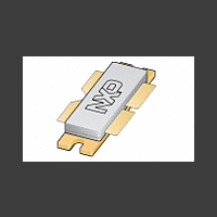
BLF888 NXP Semiconductors, BLF888 Datasheet

BLF888
Specifications of BLF888
Available stocks
Related parts for BLF888
BLF888 Summary of contents
Page 1
... BLF888 UHF power LDMOS transistor Rev. 5 — 21 January 2011 1. Product profile 1.1 General description A 500 W LDMOS RF power transistor for broadcast transmitter applications and industrial applications. The transistor is optimized for digital applications and can deliver 110 W average DVB-T broadband over the full UHF band from 470 MHz to 860 MHz. The excellent ruggedness of this device makes it ideal for digital transmitter applications ...
Page 2
... All information provided in this document is subject to legal disclaimers. Rev. 5 — 21 January 2011 UHF power LDMOS transistor Simplified outline Graphic symbol Conditions Min - 0.5 65 - © NXP B.V. 2011. All rights reserved. BLF888 sym117 Version Max Unit 104 V +11 V C +150 C ...
Page 3
... 13 3. GS(th MHz MHz MHz GS DS Conditions total device total device All information provided in this document is subject to legal disclaimers. Rev. 5 — 21 January 2011 BLF888 UHF power LDMOS transistor Typ [1] = 110 W 0.24 L(AV) Min Typ Max [1] 104 - - [1] 1.4 1 280 [ [1] = 9.5 A ...
Page 4
... PAR (of output signal) at 0.01 % probability on CCDF; PAR of input signal = 9 0.01 % probability on CCDF. Fig 1. 6.1 Ruggedness in class-AB operation The BLF888 is capable of withstanding a load mismatch corresponding to VSWR = through all phases under the following conditions: V power. Ruggedness is measured in the application circuit as described in BLF888 Product data sheet ...
Page 5
... 1.3 A; measured in a common source DS Dq narrowband 860 MHz test circuit. 2-Tone power gain and third order intermodulation distortion as function of load power; typical values © NXP B.V. 2011. All rights reserved. BLF888 001aak642 0 IMD3 (dBc) −10 −20 −30 −40 −50 −60 ...
Page 6
... IMD3 400 500 600 700 P = 250 L(AV common source broadband test circuit as described in Section 8. 2-Tone power gain and third order intermodulation distortion as function of frequency; typical values BLF888 001aak644 70 η D (%) −10 −30 −50 250 300 350 P (W) L 001aak646 −10 IMD3 (dBc) − ...
Page 7
... V and P DS L(PEP 5.565 + j0.747 5.435 + j0.752 5.303 + j0.746 5.167 + j0.730 5.030 + j0.704 4.892 + j0.668 4.754 + j0.622 4.617 + j0.567 4.481 + j0.504 BLF888 001aak648 −10 IMD shldr (dB) −20 −30 −40 −50 800 900 f (MHz) = 1.3 A; measured 600 W (DVB-T). © NXP B.V. 2011. All rights reserved. ...
Page 8
... All information provided in this document is subject to legal disclaimers. Rev. 5 — 21 January 2011 BLF888 UHF power LDMOS transistor = 50 V and P = 600 W (DVB-T). DS L(PEP 4.346 + j0.432 4 ...
Page 9
... NXP Semiconductors 7.4 Reliability Years (1) T (2) T (3) T (4) T (5) T (6) T (7) T (8) T (9) T (10) T (11) T Fig 11. BLF888 electromigration (I 8. Test information Table 9. List of components For test circuit, see Figure 12, Figure 13 Component Description B1, B2 semi rigid coax C1 multilayer ceramic chip capacitor ...
Page 10
... F/m; height = 0.76 mm; Cu (top/bottom metallization); r All information provided in this document is subject to legal disclaimers. Rev. 5 — 21 January 2011 BLF888 UHF power LDMOS transistor Remarks TDK C4532X7R1E475MT020U or capacitor of same quality. [2] TDK C570X7R1H106KT000N or capacitor of same quality. ...
Page 11
G1(test C36 R3 C34 L32 50 Ω C33 L33 B2 R4 C35 C37 G2(test) See Table 9 for a list of components. Fig 12. Class-AB common-source broadband amplifier; V C19 R1 C17 L5 L30 ...
Page 12
... Rev. 5 — 21 January 2011 UHF power LDMOS transistor 105 mm +V D1(test) + C17 R1 − C21 C19 C11 C12 C10 19 31.5 mm C20 − C22 R2 C18 + 6.5 +V D2(test) mm BLF888 001aak651 C15 C13 C8 50 Ω C14 C16 C21 001aak652 © NXP B.V. 2011. All rights reserved ...
Page 13
... European projection BLF888 SOT979A 0.25 0.010 10.29 0.25 0.51 10.03 0.405 0.010 0.020 0.395 sot979a_po Issue date 08-04-24 08-09-04 © ...
Page 14
... Objective data sheet All information provided in this document is subject to legal disclaimers. Rev. 5 — 21 January 2011 BLF888 UHF power LDMOS transistor Change notice Supersedes - BLF888 v.4 the symbol V has been changed BLF888 v.3 - BLF888 v.2 - BLF888 v © NXP B.V. 2011. All rights reserved ...
Page 15
... Export control — This document as well as the item(s) described herein may be subject to export control regulations. Export might require a prior authorization from national authorities. All information provided in this document is subject to legal disclaimers. Rev. 5 — 21 January 2011 BLF888 UHF power LDMOS transistor © NXP B.V. 2011. All rights reserved ...
Page 16
... Notice: All referenced brands, product names, service names and trademarks are the property of their respective owners. http://www.nxp.com salesaddresses@nxp.com All information provided in this document is subject to legal disclaimers. Rev. 5 — 21 January 2011 BLF888 UHF power LDMOS transistor © NXP B.V. 2011. All rights reserved ...
Page 17
... Please be aware that important notices concerning this document and the product(s) described herein, have been included in section ‘Legal information’. © NXP B.V. 2011. For more information, please visit: http://www.nxp.com For sales office addresses, please send an email to: salesaddresses@nxp.com BLF888 All rights reserved. Date of release: 21 January 2011 Document identifier: BLF888 ...


