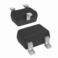
Thermal Characteristics
Electrical Characteristics
Maximum Ratings
Non-Repetitive Peak Reverse Voltage
Peak Repetitive Reverse Voltage
Working Peak Reverse Voltage
DC Blocking Voltage
RMS Reverse Voltage
Forward Continuous Current (Note 1)
Average Rectified Output Current (Note 1)
Non-Repetitive Peak Forward Surge Current
Power Dissipation (Note 1)
Thermal Resistance Junction to Ambient Air (Note 1)
Operating and Storage Temperature Range
Reverse Breakdown Voltage (Note 2)
Forward Voltage
Peak Reverse Current (Note 2)
Total Capacitance
Reverse Recovery Time
Features
•
•
•
•
•
•
Notes:
MMBD4448HW
Document number: DS30228 Rev. 7 - 2
Fast Switching Speed
Surface Mount Package Ideally Suited for Automated Insertion
For General Purpose Switching Applications
High Conductance
Lead Free/RoHS Compliant (Note 3)
"Green" Device (Notes 4 and 5)
1. Device mounted on FR-4 PCB, 1 inch x 0.85 inch x 0.062 inch; pad layout as shown on Diodes Inc. suggested pad layout
2. Short duration pulse test used to minimize self-heating effect.
3. No purposefully added lead.
4. Diodes Inc.'s "Green" policy can be found on our website at http://www.diodes.com/products/lead_free/index.php.
5. Product manufactured with Date Code 0627 (week 27, 2006) and newer are built with Green Molding Compound. Product
document AP02001, which can be found on our website at http://www.diodes.com/datasheets/ap02001.pdf.
manufactured prior to Date Code 0627 are built with Non-Green Molding Compound and may contain Halogens or Sb2O3 Fire Retardants.
Characteristic
Characteristic
Characteristic
@T
A
= 25°C unless otherwise specified
@T
A
= 25°C unless otherwise specified
TOP VIEW
@ t = 1.0μs
@ t = 1.0s
www.diodes.com
SOT-323
Symbol
V
1 of 3
(BR)R
C
V
I
t
R
rr
F
T
Mechanical Data
T
Symbol
Symbol
V
•
•
•
•
•
•
•
•
•
J
V
V
R(RMS)
R
V
I
, T
I
RWM
V
FSM
P
RRM
FM
I
RM
θ JA
O
Please click here to visit our online spice models database.
R
D
STG
Case: SOT-323
Case Material: Molded Plastic, "Green" Molding Compound,
Note 5. UL Flammability Classification Rating 94V-0
Moisture Sensitivity: Level 1 per J-STD-020D
Terminals: Solderable per MIL-STD-202, Method 208
Lead Free Plating (Matte Tin Finish annealed over
Alloy 42 leadframe).
Polarity: See Diagram
Marking Information: See Page 2
Ordering Information: See Page 2
Weight: 0.006 grams (approximate)
0.62
Min
80
⎯
⎯
⎯
⎯
⎯
⎯
Internal Schematic
TOP VIEW
0.855
Max
0.72
1.25
100
1.0
3.5
4.0
⎯
50
30
25
SURFACE MOUNT SWITCHING DIODE
-65 to +150
Value
Value
Unit
100
500
250
200
625
4.0
2.0
nA
μA
μA
nA
pF
80
57
ns
V
V
I
I
I
I
I
V
V
V
V
V
V
R
F
F
F
F
R
R
R
R
R
R
= 5.0mA
= 10mA
= 100mA
= 150mA
= 2.5μA
= 70V
= 75V, T
= 25V, T
= 20V
= 6V, f = 1.0MHz
= 6V, I
MMBD4448HW
Test Condition
F
= 5mA
J
J
= 150°C
= 150°C
© Diodes Incorporated
°C/W
Unit
Unit
mW
mA
mA
°C
V
V
V
A
March 2008