PMEG4010EP,115 NXP Semiconductors, PMEG4010EP,115 Datasheet
PMEG4010EP,115
Specifications of PMEG4010EP,115


Related parts for PMEG4010EP,115


PMEG4010EP,115 Summary of contents
Page 1
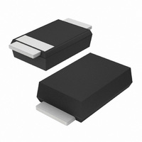
PMEG4010EP 1 A low V Rev. 02 — 15 April 2010 1. Product profile 1.1 General description Planar Maximum Efficiency General Application (MEGA) Schottky barrier rectifier with an integrated guard ring for stress protection, encapsulated in a SOD128 small and ...
Page 2
... NXP Semiconductors 2. Pinning information Table 2. Pin 1 2 [1] The marking bar indicates the cathode. 3. Ordering information Table 3. Type number PMEG4010EP 4. Marking Table 4. Type number PMEG4010EP 5. Limiting values Table 5. In accordance with the Absolute Maximum Rating System (IEC 60134). Symbol F(AV) I FSM P tot ...
Page 3
... NXP Semiconductors Table 5. In accordance with the Absolute Maximum Rating System (IEC 60134). Symbol amb T stg [1] Device mounted on a ceramic PCB °C prior to surge. [ [3] Reflow soldering is the only recommended soldering method. [4] Device mounted on an FR4 PCB, single-sided copper, tin-plated and standard footprint. ...
Page 4
... NXP Semiconductors 3 10 duty cycle = Z th(j-a) (K/ 0.5 0.33 0.25 0.2 0.1 10 0.05 0.02 0. −1 10 −3 − FR4 PCB, standard footprint Fig 1. Transient thermal impedance from junction to ambient as a function of pulse duration; typical values th(j-a) (K/W) duty cycle = 0.75 0.5 ...
Page 5
... NXP Semiconductors th(j-a) (K/W) duty cycle = 0.75 0.5 0.33 0.25 0.2 10 0.1 0.05 0.02 0. −1 10 −3 − Ceramic PCB standard footprint 2 3 Fig 3. Transient thermal impedance from junction to ambient as a function of pulse duration; typical values 7. Characteristics Table 7. ° Symbol PMEG4010EP_2 Product data sheet − ...
Page 6
... NXP Semiconductors (A) 1 (1) (2) −1 10 (3) (4) (5) −2 10 −3 10 − 0.2 0.4 = 150 °C ( 125 °C ( °C ( °C ( −40 °C ( Fig 4. Forward current as a function of forward voltage; typical values = 25 ° MHz; T amb Fig 6. Diode capacitance as a function of reverse voltage; typical values ...
Page 7
... NXP Semiconductors 0.6 P F(AV) (W) 0.4 (2) (1) 0 0.4 0.8 = 150 ° (1) δ = 0.1 (2) δ = 0.2 (3) δ = 0.5 (4) δ Fig 7. Average forward power dissipation as a function of average forward current; typical values 1.6 (1) I F(AV) (A) 1.2 (2) 0.8 (3) (4) 0 100 FR4 PCB, standard footprint = 150 °C ...
Page 8
... NXP Semiconductors 1.6 (1) I F(AV) (A) 1.2 (2) 0.8 (3) (4) 0 100 Ceramic PCB standard footprint 150 ° (1) δ (2) δ kHz (3) δ kHz (4) δ kHz Fig 11. Average forward current as a function of ambient temperature; typical values PMEG4010EP_2 Product data sheet 006aab384 1.6 I F(AV) (A) 1.2 0.8 ...
Page 9
... NXP Semiconductors 8. Test information Fig 13. Duty cycle definition The current ratings for the typical waveforms as shown in calculated according to the equations RMS 8.1 Quality information This product has been qualified in accordance with the Automotive Electronics Council (AEC) standard Q101 - Stress test qualification for discrete semiconductors, and is suitable for use in automotive applications ...
Page 10
... NXP Semiconductors 10. Packing information Table 8. The indicated -xxx are the last three digits of the 12NC ordering code. Type number PMEG4010EP [1] For further information and the availability of packing methods, see 11. Soldering 3.4 Fig 15. Reflow soldering footprint SOD128 PMEG4010EP_2 Product data sheet Packing methods ...
Page 11
... NXP Semiconductors 12. Revision history Table 9. Revision history Document ID Release date PMEG4010EP_2 20100415 • Modifications: Table 5 “Limiting • Section 13 “Legal PMEG4010EP_1 20081209 PMEG4010EP_2 Product data sheet 1 A low V Data sheet status Product data sheet values”: I maximum value amended FSM information”: updated Product data sheet All information provided in this document is subject to legal disclaimers ...
Page 12
... NXP Semiconductors and its customer, unless NXP Semiconductors and customer have explicitly agreed otherwise in writing event however, shall an agreement be valid in which the NXP Semiconductors product is deemed to offer functions and qualities beyond those described in the Product data sheet. ...
Page 13
... NXP Semiconductors 14. Contact information For more information, please visit: For sales office addresses, please send an email to: PMEG4010EP_2 Product data sheet http://www.nxp.com salesaddresses@nxp.com All information provided in this document is subject to legal disclaimers. Rev. 02 — 15 April 2010 PMEG4010EP 1 A low V MEGA Schottky barrier rectifier F © ...
Page 14
... NXP Semiconductors 15. Contents 1 Product profile . . . . . . . . . . . . . . . . . . . . . . . . . . 1 1.1 General description . . . . . . . . . . . . . . . . . . . . . 1 1.2 Features and benefits . . . . . . . . . . . . . . . . . . . . 1 1.3 Applications . . . . . . . . . . . . . . . . . . . . . . . . . . . 1 1.4 Quick reference data . . . . . . . . . . . . . . . . . . . . 1 2 Pinning information . . . . . . . . . . . . . . . . . . . . . . 2 3 Ordering information . . . . . . . . . . . . . . . . . . . . . 2 4 Marking . . . . . . . . . . . . . . . . . . . . . . . . . . . . . . . . 2 5 Limiting values Thermal characteristics . . . . . . . . . . . . . . . . . . 3 7 Characteristics . . . . . . . . . . . . . . . . . . . . . . . . . . 5 8 Test information . . . . . . . . . . . . . . . . . . . . . . . . . 9 8.1 Quality information . . . . . . . . . . . . . . . . . . . . . . 9 9 Package outline . . . . . . . . . . . . . . . . . . . . . . . . . 9 10 Packing information ...