J177,126 NXP Semiconductors, J177,126 Datasheet - Page 3
J177,126
Manufacturer Part Number
J177,126
Description
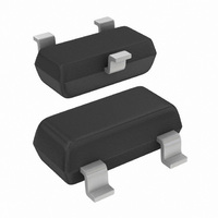
JFET P-CHAN 30V SOT-54
Manufacturer
NXP Semiconductors
Datasheet
1.PMBFJ176215.pdf
(8 pages)
Specifications of J177,126
Package / Case
TO-236-3, SC-59, SOT-23-3
Current - Drain (idss) @ Vds (vgs=0)
1.5mA @ 15V
Drain To Source Voltage (vdss)
30V
Fet Type
P-Channel
Voltage - Breakdown (v(br)gss)
30V
Voltage - Cutoff (vgs Off) @ Id
800mV @ 10nA
Input Capacitance (ciss) @ Vds
8pF @ 10V (VGS)
Resistance - Rds(on)
300 Ohm
Mounting Type
Through Hole
Power - Max
400mW
Configuration
Single
Minimum Operating Temperature
- 65 C
Mounting Style
SMD/SMT
Transistor Polarity
P-Channel
Resistance Drain-source Rds (on)
300 Ohms
Drain Source Voltage Vds
30 V
Gate-source Cutoff Voltage
0.8 V to 2.25 V
Gate-source Breakdown Voltage
30 V
Maximum Drain Gate Voltage
30 V
Continuous Drain Current
20 mA
Drain Current (idss At Vgs=0)
1.5 mA to 20 mA
Power Dissipation
300 mW
Maximum Operating Temperature
+ 150 C
Channel Type
P
Gate-source Voltage (max)
30V
Drain Current (max)
20mA
Drain-gate Voltage (max)
30V
Drain-source Volt (max)
30V
Operating Temperature (max)
150C
Operating Temperature Classification
Military
Mounting
Through Hole
Pin Count
3
Lead Free Status / RoHS Status
Lead free / RoHS Compliant
Lead Free Status / RoHS Status
Lead free / RoHS Compliant, Lead free / RoHS Compliant
Other names
934005320126
J177 AMO
J177 AMO
J177 AMO
J177 AMO


NXP Semiconductors
RATINGS
Limiting values in accordance with the Absolute Maximum System (IEC 134)
THERMAL RESISTANCE
STATIC CHARACTERISTICS
T
Note
1. Mounted on a ceramic substrate of 8 mm 10 mm 0,7 mm.
April 1995
Drain-source voltage
Gate-source voltage
Gate-drain voltage
Gate current (d.c.)
Total power dissipation
Storage temperature range
Junction temperature
From junction to ambient in free air
Gate cut-off current
Drain cut-off current
Drain current
Gate-source breakdown voltage
Gate-source cut-off voltage
Drain-source ON-resistance
j
= 25 C unless otherwise specified
P-channel silicon field-effect transistors
up to T
V
V
V
I
I
V
G
GS
D
= 1 A; V
DS
DS
DS
= 10 nA; V
= 20 V; V
= 15 V; V
= 15 V; V
= 0,1 V; V
amb
= 25 C
DS
DS
DS
= 0
GS
GS
GS
= 0
= 15 V
= 0
(1)
= 0
= 10 V
3
R
V
I
I
I
V
R
V
V
V
I
P
T
T
GSS
th j-a
(BR)GSS
GS off
stg
j
DS on
GSO
GDO
tot
DSX
DSS
G
DS
max.
max.
max.
max.
max.
max.
=
PMBFJ174
135
20
30
10
85
1
1
5
PMBFJ174 to 177
65 to 150
175
125
70
30
430
300
150
30
30
30
50
1
1
7
3
6
Product specification
176
250
35
30
1
1
2
1
4
2,25
177
300
1,5
0,8
20
30 V
1 nA
1 nA
K/W
V
V
V
mA
mW
C
C
mA
mA
V
V
Related parts for J177,126
Image
Part Number
Description
Manufacturer
Datasheet
Request
R

Part Number:
Description:
RF JFET AMMORA FET-RFSS
Manufacturer:
NXP Semiconductors
Datasheet:

Part Number:
Description:
NXP Semiconductors designed the LPC2420/2460 microcontroller around a 16-bit/32-bitARM7TDMI-S CPU core with real-time debug interfaces that include both JTAG andembedded trace
Manufacturer:
NXP Semiconductors
Datasheet:

Part Number:
Description:
NXP Semiconductors designed the LPC2458 microcontroller around a 16-bit/32-bitARM7TDMI-S CPU core with real-time debug interfaces that include both JTAG andembedded trace
Manufacturer:
NXP Semiconductors
Datasheet:
Part Number:
Description:
NXP Semiconductors designed the LPC2468 microcontroller around a 16-bit/32-bitARM7TDMI-S CPU core with real-time debug interfaces that include both JTAG andembedded trace
Manufacturer:
NXP Semiconductors
Datasheet:
Part Number:
Description:
NXP Semiconductors designed the LPC2470 microcontroller, powered by theARM7TDMI-S core, to be a highly integrated microcontroller for a wide range ofapplications that require advanced communications and high quality graphic displays
Manufacturer:
NXP Semiconductors
Datasheet:
Part Number:
Description:
NXP Semiconductors designed the LPC2478 microcontroller, powered by theARM7TDMI-S core, to be a highly integrated microcontroller for a wide range ofapplications that require advanced communications and high quality graphic displays
Manufacturer:
NXP Semiconductors
Datasheet:
Part Number:
Description:
The Philips Semiconductors XA (eXtended Architecture) family of 16-bit single-chip microcontrollers is powerful enough to easily handle the requirements of high performance embedded applications, yet inexpensive enough to compete in the market for hi
Manufacturer:
NXP Semiconductors
Datasheet:
Part Number:
Description:
The XA-S3 device is a member of Philips Semiconductors? XA(eXtended Architecture) family of high performance 16-bitsingle-chip microcontrollers
Manufacturer:
NXP Semiconductors
Datasheet:

Part Number:
Description:
The NXP BlueStreak LH75401/LH75411 family consists of two low-cost 16/32-bit System-on-Chip (SoC) devices
Manufacturer:
NXP Semiconductors
Datasheet:
Part Number:
Description:
The NXP LPC3130/3131 combine an 180 MHz ARM926EJ-S CPU core, high-speed USB2
Manufacturer:
NXP Semiconductors
Datasheet:
Part Number:
Description:
The NXP LPC3141 combine a 270 MHz ARM926EJ-S CPU core, High-speed USB 2
Manufacturer:
NXP Semiconductors
Part Number:
Description:
The NXP LPC3143 combine a 270 MHz ARM926EJ-S CPU core, High-speed USB 2
Manufacturer:
NXP Semiconductors

Part Number:
Description:
The NXP LPC3152 combines an 180 MHz ARM926EJ-S CPU core, High-speed USB 2
Manufacturer:
NXP Semiconductors