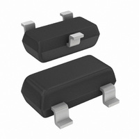
J177,126 NXP Semiconductors, J177,126 Datasheet - Page 4

J177,126
Manufacturer Part Number
J177,126
Description
JFET P-CHAN 30V SOT-54
Manufacturer
NXP Semiconductors
Datasheet
1.PMBFJ176215.pdf
(8 pages)
Specifications of J177,126
Package / Case
TO-236-3, SC-59, SOT-23-3
Current - Drain (idss) @ Vds (vgs=0)
1.5mA @ 15V
Drain To Source Voltage (vdss)
30V
Fet Type
P-Channel
Voltage - Breakdown (v(br)gss)
30V
Voltage - Cutoff (vgs Off) @ Id
800mV @ 10nA
Input Capacitance (ciss) @ Vds
8pF @ 10V (VGS)
Resistance - Rds(on)
300 Ohm
Mounting Type
Through Hole
Power - Max
400mW
Configuration
Single
Minimum Operating Temperature
- 65 C
Mounting Style
SMD/SMT
Transistor Polarity
P-Channel
Resistance Drain-source Rds (on)
300 Ohms
Drain Source Voltage Vds
30 V
Gate-source Cutoff Voltage
0.8 V to 2.25 V
Gate-source Breakdown Voltage
30 V
Maximum Drain Gate Voltage
30 V
Continuous Drain Current
20 mA
Drain Current (idss At Vgs=0)
1.5 mA to 20 mA
Power Dissipation
300 mW
Maximum Operating Temperature
+ 150 C
Channel Type
P
Gate-source Voltage (max)
30V
Drain Current (max)
20mA
Drain-gate Voltage (max)
30V
Drain-source Volt (max)
30V
Operating Temperature (max)
150C
Operating Temperature Classification
Military
Mounting
Through Hole
Pin Count
3
Lead Free Status / RoHS Status
Lead free / RoHS Compliant
Lead Free Status / RoHS Status
Lead free / RoHS Compliant, Lead free / RoHS Compliant
Other names
934005320126
J177 AMO
J177 AMO
J177 AMO
J177 AMO
NXP Semiconductors
DYNAMIC CHARACTERISTICS
T
April 1995
handbook, halfpage
Input capacitance, f = 1 MHz
Feedback capacitance, f = 1 MHz
Switching times (see Fig.2 3)
Delay time
Rise time
Turn-on time
Storage temperature
Fall time
Turn-off time
Test conditions:
j
= 25 C unless otherwise specified
P-channel silicon field-effect transistors
V
V
V
GS
GS
GS
= 10 V; V
= V
= 10 V; V
DS
Fig.2 Switching times test circuit
= 0
V in
DS
DS
= 0 V
= 0 V
50 Ω
−V DD
50 Ω
R L
D.U.T
MBK292
V out
C
C
C
t
t
t
t
t
t
V
V
R
V
d
r
on
s
f
off
4
GS off
GS on
is
is
rs
L
DD
Rise time input voltage 1 ns
OUTPUT
INPUT
typ.
typ.
typ.
PMBFJ174
typ.
typ.
typ.
typ.
typ.
typ.
V GSoff
Fig.3 Input and output waveforms
10%
t s
560
10
15
10
12
2
5
7
5
0
t
10%
t
t f
d
s
t
t
1200
175
90%
PMBFJ174 to 177
r
f
10
15
10
20
30
= t
= t
5
6
8
0
30
8
4
on
off
2000
176
Product specification
15
20
35
15
20
35
90%
6
6
0
t d
2900
177
90%
t r
20 ns
25 ns
45 ns
20 ns
25 ns
45 ns
6 V
3 V
0 V
10%
MBK293
pF
pF
pF


