FDY3000NZ Fairchild Semiconductor, FDY3000NZ Datasheet
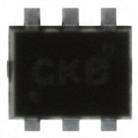
MOSFET N-CH DUAL SC89

FDY3000NZ

Manufacturer Part Number
FDY3000NZ
Description
MOSFET N-CH DUAL SC89
Manufacturer
Fairchild Semiconductor
Series
PowerTrench®r
Type
Power MOSFETr
Datasheet

Specifications of FDY3000NZ

Fet Type
2 N-Channel (Dual)
Fet Feature
Logic Level Gate
Rds On (max) @ Id, Vgs
700 mOhm @ 600mA, 4.5V
Drain To Source Voltage (vdss)
20V
Current - Continuous Drain (id) @ 25° C
600mA
Vgs(th) (max) @ Id
1.3V @ 250µA
Gate Charge (qg) @ Vgs
1.1nC @ 4.5V
Input Capacitance (ciss) @ Vds
60pF @ 10V
Power - Max
446mW
Mounting Type
Surface Mount
Package / Case
SC-89-6, SOT-666
Configuration
Dual
Transistor Polarity
N-Channel
Resistance Drain-source Rds (on)
0.7 Ohm @ 4.5 V
Forward Transconductance Gfs (max / Min)
1.8 S
Drain-source Breakdown Voltage
20 V
Gate-source Breakdown Voltage
+/- 12 V
Continuous Drain Current
0.6 A
Power Dissipation
625 mW
Maximum Operating Temperature
+ 150 C
Mounting Style
SMD/SMT
Minimum Operating Temperature
- 55 C
Number Of Elements
2
Polarity
N
Channel Mode
Enhancement
Drain-source On-res
0.7Ohm
Drain-source On-volt
20V
Gate-source Voltage (max)
±12V
Operating Temp Range
-55C to 150C
Operating Temperature Classification
Military
Mounting
Surface Mount
Pin Count
6
Package Type
SC-89
Lead Free Status / RoHS Status
Lead free / RoHS Compliant
Other names
FDY3000NZTR

Available stocks

Company
Part Number
Manufacturer
Quantity
Price
Part Number:
FDY3000NZ
Manufacturer:
Fairchild Semiconductor
Quantity:
74 306
Company:
Part Number:
FDY3000NZ
Quantity:
12 000
Company:
Part Number:
FDY3000NZ
Quantity:
30 000
FDY3000NZ
Dual N- Channel 2. 5V Speci f i ed Power Tr e nch MOSFET
Gener al Descr i pt i on
Thi s Dual N- Channel MOSFET has been des i gned
us i ng Fai rc hi l d Semi c onduc t or’ s adv anc ed Power
Trenc h proc es s t o opt i mi z e t he R
Appl i cat i ons
FDY3000NZ Rev B
2007 Fai rc hi l d Semi c onduc t or Corporat i on
Absol ut e Maxi m um Rat i ngs
Sym bol
V
V
I
P
T
Ther m al Char act er i st i cs
R
R
Package Mar ki ng and Or der i ng I nf or m at i on
Li - Ion Bat t ery Pac k
D
1
J
DSS
GSS
D
, T
JA
JA
Dev i ce Mar ki ng
STG
2
C
Drai n- Sourc e Vol t age
Gat e- Sourc e Vol t age
Drai n Current – Cont i nuous
Power Di s s i pat i on ( St eady St at e)
Operat i ng and St orage Junc t i on Temp erat ure
Range
Thermal Re s i s t anc e, Junc t i on- t o- Ambi e nt
3
– Pul s ed
FDY3000NZ
DS( ON)
Par am et er
Dev i ce
6
@ V
5
GS
= 2. 5v .
T
4
A
=25
Reel Si z e
o
C unl es s ot herwi s e not ed
7 ’ ’
( Not e 1a)
( Not e 1a)
( Not e 1b)
( Not e 1a)
( Not e 1b)
Feat ur es
600 mA, 20 V R
ESD prot ec t i on di ode ( not e 3)
RoHS Compl i ant
G
S
D
1
1
2
Tape wi dt h
–55 t o +150
1
2
3
Rat i ngs
8 mm
R
DS( ON)
DS( ON)
1000
600
625
446
200
280
20
12
= 700 m
= 850 m
January 2007
@ V
January 2007
@ V
GS
GS
3000 uni t s
www. f ai rc hi l ds emi . c om
6
5
4
Quant i t y
= 2. 5 V
= 4. 5 V
Uni t s
D
G
S
mW
mA
C/ W
V
V
C
1
2
2
tm

Related parts for FDY3000NZ

FDY3000NZ Summary of contents

Page 1

... Thermal anc e, Junc Ambi Thermal anc e, Junc Ambi Package Mar ki ng and Or der Dev i ce Mar ki ng Dev FDY3000NZ 2007 Fai Semi c onduc t or Corporat i on FDY3000NZ Rev B Feat ur es 600 mA ESD prot ode ( not e 3) RoHS Compl i ant ...

Page 2

... Q Diode Reverse Recovery Charge rr Notes the sum of the j unction-to-case and case-to-ambient thermal resistance where the case thermal reference is defined as the solder mounting surface of JA the drain pins guaranteed by design while FDY3000NZ Rev 25° C unless otherwise noted A Test Conditions 250 250 A, Referenced ...

Page 3

... Figure 3. On-Resistance Variation with Temperature 0.8 0.6 0 125 C A 0.2 -55 0 0 GATE TO SOURCE VOLTAGE (V) GS Figure 5. Transfer Characteristics. FDY3000NZ Rev B 2.6 2 2.0V GS 2.2 2.0V 2 1.8 1.6 1.4 1.2 1 0.8 0 0.75 1 Figure 2. On-Resistance Variation with Drain Current and Gate Voltage. 1 0.9 0.8 0.7 ...

Page 4

... D = 0.5 0.2 0.1 0.1 0.05 0.02 0.01 SINGLE PULSE 0.01 0.0001 0.001 Figure 11. Transient Thermal Response Curve. Thermal characterization performed using the conditions described in Note 1b. Transient thermal response will change depending on the circuit board design. FDY3000NZ Rev B 100 10V 15V rss 0 0 ...

Page 5

... Dimensional Outline and Pad Layout 1.70 1.50 6 1.20 BSC 1 (0.20) 0.20 BSC FDY3000NZ Rev B 0.30 0.50 0.15 4 1.70 1.25 1.55 3 0.30 0.50 LAND PATTERN RECOMMENDATION 1.00 0.60 SEE DETAIL A 0.56 0.35 BSC 0.10 0.00 NOTES: UNLESS OTHERWISE SPECIFIED A) THIS PACKAGE CONFORMS TO EIAJ SC89 PACKAGING STANDARD ...

Page 6

TRADEMARKS The following are registered and unregistered tradem ark s F airc hild onduc tor owns or is authoriz ed to use and is not intended haustiv e list of all suc ...

Related keywords