FDMS9600S Fairchild Semiconductor, FDMS9600S Datasheet
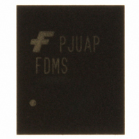
MOSFET N-CH DUAL 30V POWER56

FDMS9600S

Manufacturer Part Number
FDMS9600S
Description
MOSFET N-CH DUAL 30V POWER56
Manufacturer
Fairchild Semiconductor
Series
PowerTrench®r
Datasheet

Specifications of FDMS9600S

Fet Type
2 N-Channel (Dual)
Fet Feature
Logic Level Gate
Rds On (max) @ Id, Vgs
8.5 mOhm @ 12A, 10V
Drain To Source Voltage (vdss)
30V
Current - Continuous Drain (id) @ 25° C
12A, 16A
Vgs(th) (max) @ Id
3V @ 250µA
Gate Charge (qg) @ Vgs
13nC @ 4.5V
Input Capacitance (ciss) @ Vds
1705pF @ 15V
Power - Max
1W
Mounting Type
Surface Mount
Package / Case
8-MLP, Power56
Configuration
Dual
Transistor Polarity
N-Channel
Resistance Drain-source Rds (on)
0.0085 Ohm @ 10 V @ Q1
Drain-source Breakdown Voltage
30 V
Gate-source Breakdown Voltage
+/- 20 V
Continuous Drain Current
12 A @ Q1 or 16 A @ Q2
Power Dissipation
2500 mW
Maximum Operating Temperature
+ 150 C
Mounting Style
SMD/SMT
Minimum Operating Temperature
- 55 C
Lead Free Status / RoHS Status
Lead free / RoHS Compliant
Other names
FDMS9600STR

Available stocks

Company
Part Number
Manufacturer
Quantity
Price
Part Number:
FDMS9600S
Manufacturer:
Fairchild Semiconductor
Quantity:
27 745
Part Number:
FDMS9600S
Manufacturer:
FAIRCH
Quantity:
308
Part Number:
FDMS9600S
Manufacturer:
FAIRCHILD/仙童
Quantity:
20 000
©2008 Fairchild Semiconductor Corporation
FDMS9600S Rev.D1
FDMS9600S
Dual N-Channel PowerTrench
Q1: 30V, 32A, 8.5mΩ Q2: 30V, 30A, 5.5mΩ
Features
Q1: N-Channel
Q2: N-Channel
MOSFET Maximum Ratings
Thermal Characteristics
Package Marking and Ordering Information
V
V
I
P
T
R
R
R
D
DS
GS
D
J
θJA
θJA
θJC
Max r
Max r
Max r
Max r
Low Qg high side MOSFET
Low r
Thermally efficient dual Power 56 package
Pinout optimized for simple PCB design
RoHS Compliant
, T
Symbol
Device Marking
STG
FDMS9600S
DS(on)
DS(on)
DS(on)
DS(on)
DS(on)
low side MOSFET
= 8.5mΩ at V
= 12.4mΩ at V
= 5.5mΩ at V
= 7.0mΩ at V
Drain to Source Voltage
Gate to Source Voltage
Drain Current
Power Dissipation for Single Operation
Operating and Storage Junction Temperature Range
Thermal Resistance, Junction to Ambient
Thermal Resistance, Junction to Case
G2
G2
GS
GS
GS
GS
S2
S2
= 10V, I
= 10V, I
= 4.5V, I
FDMS9600S
= 4.5V, I
S2
S2
-Continuous (Silicon limited)
-Continuous
-Pulsed
Device
-Continuous (Package limited) T
S2
S2
Power 56
D
D
D
S1/D2
S1/D2
D
= 12A
= 16A
= 14A
= 10A
T
A
D1
D1
G1
G1
= 25°C unless otherwise noted
Parameter
D1
D1
®
D1
D1
Power 56
Package
MOSFET
D1
D1
1
T
T
C
C
A
General Description
This device includes two specialized MOSFETs in a unique dual
Power 56 package.
Synchronous Buck power stage in terms of efficiency and PCB
utilization. The low switching loss "High Side" MOSFET is com-
plemented by a Low Conduction Loss "Low Side" SyncFET.
Applications
Synchronous Buck Converter for:
= 25°C
= 25°C
= 25°C
Notebook System Power
General Purpose Point of Load
Reel Size
13”
5
6
7
8
(Note 1a)
(Note 1b)
(Note 1a)
(Note 1a)
(Note 1b)
Q2
It is designed to provide an optimal
Tape Width
±20
Q1
12mm
30
32
55
12
60
Q 1
3
-55 to +150
120
1.0
2.5
50
4
3
2
1
September 2008
±20
108
Q2
1.2
30
30
16
60
www.fairchildsemi.com
3000 units
Quantity
Units
°C/W
°C
W
V
V
A
tm

Related parts for FDMS9600S

FDMS9600S Summary of contents

Page 1

... Thermal Resistance, Junction to Case θJC Package Marking and Ordering Information Device Marking Device FDMS9600S FDMS9600S ©2008 Fairchild Semiconductor Corporation FDMS9600S Rev.D1 ® MOSFET General Description This device includes two specialized MOSFETs in a unique dual Power 56 package. = 12A D Synchronous Buck power stage in terms of efficiency and PCB ...

Page 2

... Rise Time r t Turn-Off Delay Time d(off) t Fall Time f Q Total Gate Charge g(TOT) Q Gate to Source Gate Charge gs Q Gate to Drain “Miller” Charge gd FDMS9600S Rev. 25°C unless otherwise noted J Test Conditions I = 250µ 1mA 250µA, referenced to 25° 1mA, referenced to 25° ...

Page 3

... SD t Reverse Recovery Time rr Q Reverse Recovery Charge rr Notes determined with the device mounted on a 1in θJA the user's board design. 2: Pulse Test: Pulse Width < 300µs, Duty cycle < 2.0%. FDMS9600S Rev. 25°C unless otherwise noted J Test Conditions 2.1A (Note 0V ...

Page 4

... JUNCTION TEMPERATURE J Figure 3. Normalized On-Resistance vs Junction Temperature 60 PULSE DURATION = 300 s µ DUTY CYCLE = 2.0%MAX =125 1.0 1.5 2 GATE TO SOURCE VOLTAGE (V) GS Figure 5. Transfer Characteristics FDMS9600S Rev. 25°C unless otherwise noted J PULSE DURATION = 300 s µ DUTY CYCLE = 2.0%MAX 1.5 2.0 75 100 125 150 ...

Page 5

... DRAIN to SOURCE VOLTAGE (V) DS Figure 9. Forward Bias Safe Operating Area 2 1 DUTY CYCLE-DESCENDING ORDER D = 0.5 0.2 0.1 0.05 0.1 0.02 0.01 0.01 SINGLE PULSE 0.002 - FDMS9600S Rev. 25°C unless otherwise noted J 2000 1000 V = 15V DD 100 300 100 1ms 10ms 10 100ms 1s 10s DC 0 ...

Page 6

... T , JUNCTION TEMPERATURE J Figure 14. Normalized On-Resistance vs Junction Temperature 60 PULSE DURATION = 300 s µ DUTY CYCLE = 2.0%MAX =125 1.0 1.5 2.0 2 GATE TO SOURCE VOLTAGE (V) GS Figure 16. Transfer Characteristics FDMS9600S Rev. µ 0.6 0.8 1.0 Figure 13. Normalized on-Resistance vS Drain 75 100 125 150 0. - 1E-3 3.0 3 ...

Page 7

... Typical Characteristics 16A =10V GATE CHARGE(nC) g Figure 18. Gate Charge Characteristics FDMS9600S Rev. 15V DD = 20V 5000 1000 f = 1MHz 100 0 DRAIN TO SOURCE VOLTAGE (V) DS Figure 19. Capacitance vs Drain to Source Voltage C iss C oss C rss 30 10 www.fairchildsemi.com ...

Page 8

... Dimensional Outline and Pad Layout FDMS9600S Rev.D1 8 www.fairchildsemi.com ...

Page 9

... TRADEMARKS The following includes registered and unregistered trademarks and service marks, owned by Fairchild Semiconductor and/or its global subsidiaries, and is not intended exhaustive list of all such trademarks. Build it Now™ CorePLUS™ CorePOWER™ CROSSVOLT™ CTL™ Current Transfer Logic™ ...

Related keywords