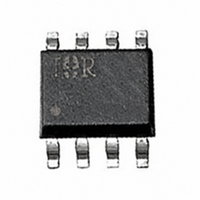
IRF7509TRPBF International Rectifier, IRF7509TRPBF Datasheet - Page 6

IRF7509TRPBF
Manufacturer Part Number
IRF7509TRPBF
Description
MOSFET N/P-CH 30V MICRO8
Manufacturer
International Rectifier
Series
HEXFET®r
Datasheet
1.IRF7509TRPBF.pdf
(8 pages)
Specifications of IRF7509TRPBF
Fet Type
N and P-Channel
Fet Feature
Logic Level Gate
Rds On (max) @ Id, Vgs
110 mOhm @ 1.7A, 10V
Drain To Source Voltage (vdss)
30V
Current - Continuous Drain (id) @ 25° C
2.7A, 2A
Vgs(th) (max) @ Id
1V @ 250µA
Gate Charge (qg) @ Vgs
12nC @ 10V
Input Capacitance (ciss) @ Vds
210pF @ 25V
Power - Max
1.25W
Mounting Type
Surface Mount
Package / Case
Micro8™
Transistor Polarity
N and P-Channel
Resistance Drain-source Rds (on)
175 mOhms
Drain-source Breakdown Voltage
30 V
Gate-source Breakdown Voltage
20 V
Continuous Drain Current
2.4 A
Power Dissipation
1.25 W
Gate Charge Qg
7.8 nC
Lead Free Status / RoHS Status
Lead free / RoHS Compliant
Other names
IRF7509TRPBF
IRF7509TRPBFTR
IRF7509TRPBFTR
Available stocks
Company
Part Number
Manufacturer
Quantity
Price
Part Number:
IRF7509TRPBF
Manufacturer:
IR
Quantity:
20 000
Fig 17. Typical On-Resistance Vs. Gate
6
Fig 19. Typical Capacitance Vs.
400
300
200
100
.6
.5
.4
.3
.2
.1
0
1
3
Drain-to-Source Voltage
Fig 21. Maximum Effective Transient Thermal Impedance, Junction-to-Ambient
C
C
C
-V
V
iss
oss
rss
DS
5
V
C
C
C
6
, Drain-to-Source Voltage (V)
GS
iss
rss
oss
1000
, Gate to Source Voltage (V)
100
0.1
10
0.00001
= 0V,
= C
= C
= C
1
Voltage
D = 0.50
gs
gd
ds
I
0.20
0.10
0.05
0.02
0.01
+ C
+ C
10
= -2.0
9
gd
gd
f = 1MHz
, C
(THERMAL RESPONSE)
0.0001
ds
SINGLE PULSE
12
SHORTED
100
0.001
15
A
t , Rectangular Pulse Duration (sec)
1
N-P - Channel
0.01
0.1
Fig 18. Maximum Safe Operating Area
100
0.1
10
1. Duty factor D = t / t
2. Peak T = P
20
16
12
Notes:
1
Fig 20. Typical Gate Charge Vs.
8
4
0
1
0
T
T
Single Pulse
I
C
J
D
= 25 C
= 150 C
= -1.2A
1
J
OPERATION IN THIS AREA LIMITED
-V
Gate-to-Source Voltage
DS
2
°
Q , Total Gate Charge (nC)
DM
°
, Drain-to-Source Voltage (V)
G
x Z
1
thJA
4
P
2
DM
BY R
V
V
+ T
10
DS
DS
A
t
10
1
DS(on)
6
= -15V
= -24V
t
2
FOR TEST CIRCUIT
SEE FIGURE 9
8
10us
100us
1ms
10ms
100
www.irf.com
10
100
12
A


