ZXMN6A11DN8TC Diodes Zetex, ZXMN6A11DN8TC Datasheet
ZXMN6A11DN8TC
Specifications of ZXMN6A11DN8TC
Available stocks


Related parts for ZXMN6A11DN8TC


ZXMN6A11DN8TC Summary of contents
Page 1
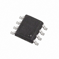
ZXMN6A11DN8 60V SO8 Dual N-channel enhancement mode MOSFET Summary (BR)DSS DS(on) 0.120 @ 0.180 @ V GS Description This new generation trench MOSFET from Zetex features a unique structure combining the benefits of ...
Page 2
Absolute maximum ratings Parameter Drain-source voltage Gate-source voltage Continuous drain current @ (c) Pulsed drain current Continuous source current (body diode) Pulsed source current (body diode) Power dissipation at T =25°C amb Linear derating factor ...
Page 3
Typical characteristics Issue 3 - September 2006 © Zetex Semiconductors plc 2006 ZXMN6A11DN8 3 www.zetex.com ...
Page 4
Electrical characteristics (at T Parameter Static Drain-source breakdown voltage V Zero gate voltage drain current Gate-body leakage Gate-source threshold voltage Static drain-source on-state (*) resistance (*)(‡) Forward transconductance (‡) Dynamic Input capacitance Output capacitance Reverse transfer capacitance (†) (‡) Switching ...
Page 5
Typical characteristics Issue 3 - September 2006 © Zetex Semiconductors plc 2006 ZXMN6A11DN8 5 www.zetex.com ...
Page 6
Typical characteristics Charge Basic gate charge waveform V DS 90% 10 d(on (on) Switching time waveforms Issue 3 - September 2006 © Zetex Semiconductors plc 2006 ...
Page 7
Issue 3 - September 2006 © Zetex Semiconductors plc 2006 Intentionally left blank 7 ZXMN6A11DN8 www.zetex.com ...
Page 8
Package outline - SO8 DIM Inches Min. Max. A 0.053 0.069 A1 0.004 0.010 D 0.189 0.197 H 0.228 0.244 E 0.150 0.157 L 0.016 0.050 Note: Controlling dimensions are in inches. Approximate dimensions are provided in millimeters Europe Americas ...