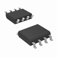
SI4559ADY-T1-GE3 Vishay, SI4559ADY-T1-GE3 Datasheet

SI4559ADY-T1-GE3
Specifications of SI4559ADY-T1-GE3
Available stocks
Related parts for SI4559ADY-T1-GE3
SI4559ADY-T1-GE3 Summary of contents
Page 1
... Top View Ordering Information: Si4559ADY-T1-E3 (Lead (Pb)-free) Si4559ADY-T1-GE3 (Lead (Pb)-free and Halogen-free) ABSOLUTE MAXIMUM RATINGS T Parameter Drain-Source Voltage Gate-Source Voltage Continuous Drain Current (T = 150 °C) J Pulsed Drain Current (10 µs Pulse Width) Source Drain Current Diode Current Pulsed Source-Drain Current Single Pulse Avalanche Current ...
Page 2
... Si4559ADY Vishay Siliconix SPECIFICATIONS °C, unless otherwise noted J Parameter Static Drain-Source Breakdown Voltage V Temperature Coefficient DS V Temperature Coefficient GS(th) Gate Threshold Voltage Gate-Body Leakage Zero Gate Voltage Drain Current b On-State Drain Current b Drain-Source On-State Resistance b Forward Transconductance a Dynamic Input Capacitance Output Capacitance ...
Page 3
... N-Channel = 8.8 Ω ≅ 3 GEN g P-Channel t d(off) = 12.5 Ω ≅ GEN ° 1 N-Channel 1.7 A, dI/dt = 100 A/µ P-Channel dI/ 100 A/µ Si4559ADY Vishay Siliconix a Typ. Min. Max N-Ch 65 100 = 1 Ω P-Ch 70 105 N- P- Ω Ω Ω N-Ch 2 ...
Page 4
... Si4559ADY Vishay Siliconix N-CHANNEL TYPICAL CHARACTERISTICS 25 °C, unless otherwise noted thru 0.0 0.2 0.4 0.6 0.8 1 Drain-to-Source Voltage (V) DS Output Characteristics 0.080 0.075 0.070 0.065 0.060 0.055 0.050 0.045 0.040 Drain Current (A) D On-Resistance vs. Drain Current and Gate Voltage 4.3 A ...
Page 5
... D 75 100 125 150 100 Limited DS(on 0 °C A Single Pulse 0.01 0.001 0 Drain-to-Source Voltage (V) DS > minimum V at which DS(on) Safe Operating Area Si4559ADY Vishay Siliconix 0.12 0.11 0.10 0.09 0. 0.06 0.05 0. Gate-to-Source V oltage (V) GS On-Resistance vs. Gate-to-Source Voltage 0.01 0 Time (s) Single Pulse Power, Junction-to-Ambient 100 µ ...
Page 6
... Si4559ADY Vishay Siliconix N-CHANNEL TYPICAL CHARACTERISTICS 25 °C, unless otherwise noted 100 T - Case Temperature (°C) C Current Derating* * The power dissipation P is based dissipation limit for cases where additional heatsinking is used used to determine the current rating, when this rating falls below the package limit ...
Page 7
... Single Pulse 0. Document Number: 73624 S09-0393-Rev. B, 09-Mar- Square Wave Pulse Duration (s) Normalized Thermal Transient Impedance, Junction-to-Ambient - Square Wave Pulse Duration (s) Normalized Thermal Transient Impedance, Junction-to-Case Si4559ADY Vishay Siliconix Notes Duty Cycle Per Unit Base = °C/W thJA ( ...
Page 8
... Si4559ADY Vishay Siliconix P-CHANNEL TYPICAL CHARACTERISTICS 25 °C, unless otherwise noted thru Drain-to-Source Voltage (V) DS Output Characteristics 0.40 0.35 0.30 0. 0.15 0.10 0.05 0. Drain Current (A) D On-Resistance vs. Drain Current 3 Total Gate Charge (nC) g Gate Charge www.vishay.com 1000 125 ° ° ° ...
Page 9
... Limited DS(on D(on) Limited 0 °C A Single Pulse BVDSS Limited 0.01 0 Drain-to-Source Voltage (V) DS > minimum V at which DS(on) Safe Operating Area, Junction-to-Case Si4559ADY Vishay Siliconix Gate-to-Source Voltage (V) GS On-Resistance vs. Gate-to-Source Voltage Time (s) Single Pulse Power Limited P(t) = 0.0001 P(t) = 0.001 P(t) = 0.01 P( ...
Page 10
... Si4559ADY Vishay Siliconix P-CHANNEL TYPICAL CHARACTERISTICS 25 °C, unless otherwise noted 4.5 4.0 3.5 3.0 2.5 2.0 1.5 1.0 0.5 0 Case Temperature (°C) C Power Derating, Junction-to-Foot * The power dissipation P is based dissipation limit for cases where additional heatsinking is used used to determine the current rating, when this rating falls below the package limit ...
Page 11
... Technology and Package Reliability represent a composite of all qualified locations. For related documents such as package/tape drawings, part marking, and reliability data, see www.vishay.com/ppg?73624. Document Number: 73624 S09-0393-Rev. B, 09-Mar- Square Wave Pulse Duration (s) Normalized Thermal Transient Impedance, Junction-to-Ambient - Square Wave Pulse Duration (s) Normalized Thermal Transient Impedance, Junction-to-Foot Si4559ADY Vishay Siliconix Notes Duty Cycle Per Unit Base = °C/W ...
Page 12
... Vishay product could result in personal injury or death. Customers using or selling Vishay products not expressly indicated for use in such applications their own risk and agree to fully indemnify and hold Vishay and its distributors harmless from and against any and all claims, liabilities, expenses and damages arising or resulting in connection with such use or sale, including attorneys fees, even if such claim alleges that Vishay or its distributor was negligent regarding the design or manufacture of the part ...


