SI4916DY-T1-E3 Vishay, SI4916DY-T1-E3 Datasheet - Page 2
SI4916DY-T1-E3
Manufacturer Part Number
SI4916DY-T1-E3
Description
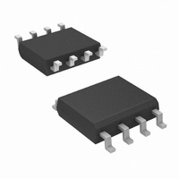
MOSFET DUAL N-CH 30V 8-SOIC
Manufacturer
Vishay
Datasheet
1.SI4916DY-T1-E3.pdf
(10 pages)
Specifications of SI4916DY-T1-E3
Transistor Polarity
N-Channel
Fet Type
2 N-Channel (Dual)
Fet Feature
Logic Level Gate
Rds On (max) @ Id, Vgs
18 mOhm @ 10A, 10V
Drain To Source Voltage (vdss)
30V
Current - Continuous Drain (id) @ 25° C
7.5A, 7.8A
Vgs(th) (max) @ Id
3V @ 250µA
Gate Charge (qg) @ Vgs
10nC @ 4.5V
Power - Max
1.9W, 2W
Mounting Type
Surface Mount
Package / Case
8-SOIC (3.9mm Width)
Minimum Operating Temperature
- 55 C
Configuration
Dual
Resistance Drain-source Rds (on)
0.018 Ohm @ 10 V
Drain-source Breakdown Voltage
30 V
Gate-source Breakdown Voltage
20 V
Continuous Drain Current
7.5 A @ Channel 1 or 7.8 A @ Channel 2
Power Dissipation
1900 mW @ Channel 1 or 2000 mW @ Channel 2
Maximum Operating Temperature
+ 150 C
Mounting Style
SMD/SMT
Continuous Drain Current Id
7.5A
Drain Source Voltage Vds
30V
On Resistance Rds(on)
14.5mohm
Rds(on) Test Voltage Vgs
20V
Lead Free Status / RoHS Status
Lead free / RoHS Compliant
Lead Free Status / RoHS Status
Lead free / RoHS Compliant, Lead free / RoHS Compliant
Other names
SI4916DY-T1-E3TR
Available stocks
Company
Part Number
Manufacturer
Quantity
Price
Company:

Part Number:
SI4916DY-T1-E3
Manufacturer:
VISHAY
Quantity:
12 956
Part Number:
SI4916DY-T1-E3
Manufacturer:
VISHAY/威世
Quantity:
20 000


Si4916DY
Vishay Siliconix
Notes:
a. Surface Mounted on 1" x 1" FR4 board.
b. Maximum under Steady State conditions is 112 °C/W for Channel 1 and 107 °C/W for Channel 2.
www.vishay.com
2
THERMAL RESISTANCE RATINGS
Parameter
Maximum Junction-to-Ambient
Maximum Junction-to-Foot (Drain)
MOSFET SPECIFICATIONS T
Parameter
Static
Drain-Source Breakdown Voltage
V
V
Gate Threshold Voltage
Gate-Body Leakage
Zero Gate Voltage Drain Current
On-State Drain Current
Drain-Source On-State Resistance
Forward Transconductance
Diode Forward Voltage
Dynamic
Total Gate Charge
Gate-Source Charge
Gate-Drain Charge
Gate Resistance
DS
GS(th)
Temperature Coefficient
Temperature Coefficient
a
b
b
b
a
b
ΔV
Symbol
ΔV
R
V
GS(th)
I
I
I
V
DS(on)
V
GS(th)
D(on)
Q
Q
GSS
DSS
DS
g
Q
R
J
DS
SD
fs
gs
gd
g
g
= 25 °C, unless otherwise noted
/T
Steady State
/T
J
J
t ≤ 10 s
V
DS
V
V
DS
DS
= 15 V, V
= 15 V, V
= 30 V, V
V
V
V
V
V
V
V
V
V
V
V
I
DS
GS
DS
GS
GS
GS
S
DS
DS
DS
I
GS
DS
S
= 1.7 A, V
= V
= 1 A, V
= 10 V, I
= 15 V, I
Symbol
= 0 V, I
= 4.5 V, I
= 4.5 V, I
= 0 V, V
= 30 V, V
= 5 V, V
I
= 10 V, I
= 15 V, I
R
R
D
Channel-1
Channel-2
GS
Test Conditions
thJA
thJF
GS
= 250 µA
GS
GS
= 4.5 V, I
, I
= 4.5 V, I
= 0 V, T
D
D
GS
GS
GS
D
D
GS
= 250 µA
D
D
D
D
= 250 µA
GS
= 10.5 A
= 10.5 A
= 10 A
= 8.5 A
= 9.3 A
= 10 A
= 0 V
= 10 V
= 20 V
= 0 V
= 0 V
D
J
D
= - 10.5 A
Typ.
= 85 °C
54
32
= 10 A
Channel-1
Ch-1
Ch-2
Ch-1
Ch-2
Ch-1
Ch-2
Ch-1
Ch-2
Ch-1
Ch-2
Ch-1
Ch-2
Ch-1
Ch-2
Ch-1
Ch-2
Ch-1
Ch-2
Ch-1
Ch-2
Ch-1
Ch-2
Ch-1
Ch-2
Ch-1
Ch-2
Ch-1
Ch-2
Ch-1
Ch-2
Ch-1
Ch-2
Max.
65
38
Min.
1.5
1.5
0.5
0.5
30
30
20
20
Typ.
47
30
0.0145
Channel-2
Typ.
0.015
0.019
0.018
S09-0540-Rev. B, 06-Apr-09
0.75
0.47
6.6
8.9
2.9
3.4
2.3
2.4
1.9
2.3
24
25
- 6
- 6
30
35
Document Number: 74331
a
Max.
0.018
0.018
0.023
0.022
60
35
Max.
2000
100
100
100
3.0
2.7
1.1
0.5
2.9
3.5
15
10
14
1
mV/°C
°C/W
Unit
Unit
nA
µA
nC
Ω
Ω
V
V
A
S
V
Related parts for SI4916DY-T1-E3
Image
Part Number
Description
Manufacturer
Datasheet
Request
R

Part Number:
Description:
Dual N-channel 30-v Mosfet With Schottky Diode
Manufacturer:
Vishay
Datasheet:
Part Number:
Description:
DUAL N-CH 30-V(D-S)MOSFET+SCHOTTKY DIODE
Manufacturer:
Vishay
Part Number:
Description:
357-036-542-201 CARDEDGE 36POS DL .156 BLK LOPRO
Manufacturer:
Vishay
Datasheet:
Part Number:
Description:
357-036-542-201 CARDEDGE 36POS DL .156 BLK LOPRO
Manufacturer:
Vishay
Datasheet:
Part Number:
Description:
357-036-542-201 CARDEDGE 36POS DL .156 BLK LOPRO
Manufacturer:
Vishay
Datasheet:
Part Number:
Description:
357-036-542-201 CARDEDGE 36POS DL .156 BLK LOPRO
Manufacturer:
Vishay
Datasheet:
Part Number:
Description:
357-036-542-201 CARDEDGE 36POS DL .156 BLK LOPRO
Manufacturer:
Vishay
Datasheet:
Part Number:
Description:
357-036-542-201 CARDEDGE 36POS DL .156 BLK LOPRO
Manufacturer:
Vishay
Datasheet:
Part Number:
Description:
357-036-542-201 CARDEDGE 36POS DL .156 BLK LOPRO
Manufacturer:
Vishay
Datasheet:
Part Number:
Description:
357-036-542-201 CARDEDGE 36POS DL .156 BLK LOPRO
Manufacturer:
Vishay
Datasheet:
Part Number:
Description:
357-036-542-201 CARDEDGE 36POS DL .156 BLK LOPRO
Manufacturer:
Vishay
Datasheet:
Part Number:
Description:
357-036-542-201 CARDEDGE 36POS DL .156 BLK LOPRO
Manufacturer:
Vishay
Datasheet:
Part Number:
Description:
357-036-542-201 CARDEDGE 36POS DL .156 BLK LOPRO
Manufacturer:
Vishay
Datasheet:
Part Number:
Description:
357-036-542-201 CARDEDGE 36POS DL .156 BLK LOPRO
Manufacturer:
Vishay
Datasheet:
Part Number:
Description:
357-036-542-201 CARDEDGE 36POS DL .156 BLK LOPRO
Manufacturer:
Vishay
Datasheet: