IRF7106 International Rectifier, IRF7106 Datasheet
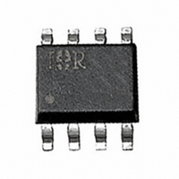
HEX/MOS N/P-CH DL 20/-20V 8-SOIC

IRF7106

Manufacturer Part Number
IRF7106
Description
HEX/MOS N/P-CH DL 20/-20V 8-SOIC
Manufacturer
International Rectifier
Series
HEXFET®r
Datasheet

Specifications of IRF7106

Fet Type
N and P-Channel
Fet Feature
Standard
Rds On (max) @ Id, Vgs
125 mOhm @ 1A, 10V
Drain To Source Voltage (vdss)
20V
Current - Continuous Drain (id) @ 25° C
3A, 2.5A
Vgs(th) (max) @ Id
1V @ 250µA
Gate Charge (qg) @ Vgs
25nC @ 10V
Input Capacitance (ciss) @ Vds
300pF @ 15V
Power - Max
2W
Mounting Type
Surface Mount
Package / Case
8-SOIC (3.9mm Width)
Lead Free Status / RoHS Status
Contains lead / RoHS non-compliant

Available stocks

Company
Part Number
Manufacturer
Quantity
Price
Part Number:
IRF7106
Manufacturer:
IR
Quantity:
20 000
Part Number:
IRF7106TRPBF
Manufacturer:
IR
Quantity:
20 000
HEXFET
Description
Fourth Generation HEXFETs from International Rectifier utilize advanced
processing techniques to achieve the lowest possible on-resistance per silicon
area. This benefit, combined with the fast switching speed and ruggedized device
design for which HEXFET Power MOSFETs are well known, provides the designer
with an extremely efficient device for use in a wide variety of applications.
The SO-8 has been modified through a customized leadframe for enhanced
thermal characteristics and multiple-die capability making it ideal in a variety of
power applications. With these improvements, multiple devices can be used in an
application with dramatically reduced board space. The package is designed for
vapor phase, infra-red, or wave soldering techniques. Power dissipation of greater
than 0.8W is possible in a typical PCB mount application.
Thermal Resistance
Absolute Maximum Ratings
** When mounted on 1" square PCB (FR-4 or G-10 Material).
R
I
I
I
P
V
dv/dt
T
D
D
DM
D
GS
J,
JA
@ T
@ T
Advanced Process Technology
Ultra Low On-Resistance
Dual N and P Channel Mosfet
Surface Mount
Available in Tape & Reel
Dynamic dv/dt Rating
Fast Switching
@T
T
For recommended footprint and soldering techniques refer to application note #AN-994.
STG
C
C
C
= 25°C
= 70°C
= 25°C
®
Power MOSFET
Junction-to-Ambient (PCB Mount)**
Continuous Drain Current, V
Pulsed Drain Current
Power Dissipation
Linear Derating Factor
Gate-to-Source Voltage
Peak Diode Recovery dv/dt
Junction and Storage Temperature Range
Parameter
Parameter
PRELIMINARY
GS
GS
@ 10V
@ 10V
G2
G1
S2
S1
69
N-CHANNEL MOSFET
P-CHANNEL MOSFET
1
2
3
4
Top View
Min.
––––
N-Channel
3.0
2.5
3.0
10
8
7
6
5
D1
D1
D2
D2
-55 to + 150
Max.
0.016
± 20
Typ.
––––
2.0
R
V
DS(on)
IRF7106
DSS
I
D
P-Channel
-2.5
-2.0
-3.0
PD - 9.1098B
-10
SO-8
0.125
N-Ch
Max.
3.0A
20V
62.5
Revision 3
0.20
-2.5A
P-Ch
-20V
Units
Units
°C/W
W/°C
V/ns
W
°C
A
V

Related parts for IRF7106

IRF7106 Summary of contents

Page 1

... For recommended footprint and soldering techniques refer to application note #AN-994. PRELIMINARY N-CHANNEL MOSFET P-CHANNEL MOSFET Top View N-Channel @ 10V 3 10V 2 3.0 Min. –––– 9.1098B IRF7106 N-Ch P- 20V -20V DSS D2 R 0.125 0.20 DS(on 3.0A -2.5A D SO-8 Max. Units P-Channel -2.5 -2.0 A -10 W 2.0 0.016 W/° ...

Page 2

... IRF7106 Electrical Characteristics @ T Parameter V Drain-to-Source Breakdown Voltage (BR)DSS Breakdown Voltage Temp. Coefficient (BR)DSS J R Static Drain-to-Source On-Resistance DS(ON) V Gate Threshold Voltage GS(th) g Forward Transconductance fs I Drain-to-Source Leakage Current DSS I Gate-to-Source Forward Leakage GSS Q Total Gate Charge g Q Gate-to-Source Charge gs Q Gate-to-Drain ("Miller") Charge ...

Page 3

... Fig 2. Typical Output Characteristics, 2 3.0A D 1.5 1.0 0.5 0 -60 -40 Fig 4. Normalized On-Resistance Vs. Temperature 2. 10V 100 Fig 6. Typical Gate Charge Vs. Gate-to-Source Voltage 71 IRF7106 VGS 15V 10V 8.0V 7.0V 6.0V 5.5V 5.0V 4.5V 20µs PULSE WIDTH T = 150° 0 100 V , Drain-to-Source Voltage ( 150 10V ...

Page 4

... IRF7106 100 150° 25° 0.1 0.4 0.6 0.8 1 Source-to-Drain Voltage (V) SD Fig 7. Typical Source-Drain Diode Forward Voltage 3.0 2.5 2.0 1.5 1.0 0.5 0 100 T , Ambient Temperature (°C) A Fig 9. Maximum Drain Current Vs. Ambient Temperature Fig 11a. Gate Charge Test Circuit N-Channel ...

Page 5

... T , Junction Temperature (°C) J Fig 15. Normalized On-Resistance Vs. Temperature -2. -10V 100 Total Gate Charge (nC) G Fig 17. Typical Gate Charge Vs. Gate-to-Source Voltage 73 IRF7106 -4.5V 20µs PULSE WIDTH T = 150° 100 , Drain-to-Source Voltage ( 150 -10V 100 120 140 160 FOR TEST CIRCUIT SEE FIGURE ...

Page 6

... IRF7106 150° 25° 0.1 0.0 1.0 2 Source-to-Drain Voltage (V) SD Fig 18. Typical Source-Drain Diode Forward Voltage 2.5 2.0 1.5 1.0 0.5 0 100 T , Ambient Temperature (°C) A Fig 20. Maximum Drain Current Vs. Ambient Temperature Fig 22a. Gate Charge Test Circuit P-Channel 100 Single Pulse ...

Page 7

... Appendix A: Figure 24, Peak Diode Recovery dv/dt Test Circuit — See page 329. Appendix B: Package Outline Mechanical Drawing — See page 332. Appendix C: Part Marking Information — See page 332. Appendix D: Tape and Reel Information — See page 336. N-P Channel 0.01 0 Rectangular Pulse Duration (sec IRF7106 ...

Related keywords