IRF5852 International Rectifier, IRF5852 Datasheet

IRF5852
Specifications of IRF5852
Available stocks
Related parts for IRF5852
IRF5852 Summary of contents
Page 1
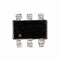
... This Dual TSOP-6 package is ideal for applications where printed circuit board space premium and where maximum functionality is required. With two die per package, the IRF5852 can provide the functionality of two SOT-23 packages in a smaller footprint. Its unique thermal design and R reduction enables an increase in current-handling capability ...
Page 2
... IRF5852 Electrical Characteristics @ T Parameter V Drain-to-Source Breakdown Voltage (BR)DSS Breakdown Voltage Temp. Coefficient (BR)DSS J R Static Drain-to-Source On-Resistance DS(on) V Gate Threshold Voltage GS(th) g Forward Transconductance fs I Drain-to-Source Leakage Current DSS Gate-to-Source Forward Leakage Gate-to-Source Reverse Leakage Q Total Gate Charge g Q Gate-to-Source Charge ...
Page 3
... V Fig 2. Typical Output Characteristics 2 1.5 ° 150 C J 1.0 0.5 0.0 3.0 -60 -40 -20 Fig 4. Normalized On-Resistance IRF5852 VGS 7.5V 4.5V 3.5V 3.0V 2.5V 2.0V 1.75V 1.5V 1.50V 20µs PULSE WIDTH T = 150 C ° Drain-to-Source Voltage ( ...
Page 4
... IRF5852 600 1MHz iss rss gd 500 oss iss 400 300 200 100 C oss C rss Drain-to-Source Voltage (V) DS Fig 5. Typical Capacitance Vs. Drain-to-Source Voltage 100 150 C ° ° 0.1 0.4 0.6 0.8 1.0 V ,Source-to-Drain Voltage (V) SD Fig 7. Typical Source-Drain Diode Forward Voltage ...
Page 5
... RESPONSE) 0.1 0.00001 0.0001 Fig 10. Typical Effective Transient Thermal Impedance, Junction-to-Ambient www.irf.com Fig 10a. Switching Time Test Circuit V DS 90% 125 150 ° 10 d(on) Fig 10b. Switching Time Waveforms 1. Duty factor Peak 0.001 0. Rectangular Pulse Duration (sec) 1 IRF5852 + - d(off Notes thJA A 0.1 ...
Page 6
... IRF5852 0.14 0.12 0. 2.7A 0.08 0.06 2.0 3.0 4.0 5.0 V GS, Gate -to -Source Voltage (V) Fig 11. Typical On-Resistance Vs. Gate Voltage Charge Fig 13a. Basic Gate Charge Waveform 6 0.30 0.20 0.10 0.00 0 6.0 7.0 8.0 Fig 12. Typical On-Resistance Vs. Drain 12V V GS Fig 13b. Gate Charge Test Circuit ...
Page 7
... Temperature ( °C ) Fig 14. Threshold Voltage Vs. Tempera- ture www.irf.com 250µ 0.001 75 100 125 150 IRF5852 0.010 0.100 1.000 10.000 Time (sec) Typical Power Vs. Time 7 ...
Page 8
... IRF5852 8 www.irf.com ...
Page 9
... EXAMPLE: T HIS I3443DV PART NUMBER WAFER LOT NUMBER CODE PART NUMBER CODE REFERENCE SI3443DV 3B = IRF5800 3C = IRF5850 3D = IRF5851 3E = IRF5852 3I = IRF5805 3J = IRF5806 DATE CODE EXAMPLES: YWW = 9603 = 6C YWW = 9632 = FF Notes : T his part marking information applies to devices produced after 02/26/2001 PART NUMBER PART NUMB ER CODE REFERENCE: ...


