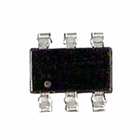
IRF5851TR International Rectifier, IRF5851TR Datasheet

IRF5851TR
Specifications of IRF5851TR
Available stocks
Related parts for IRF5851TR
IRF5851TR Summary of contents
Page 1
... Available in Tape & Reel l Low Gate Charge Description These N and P channel MOSFETs from International Rectifier utilize advanced processing techniques to achieve the extremely low on-resistance per silicon area. This benefit provides the designer with an extremely efficient device for use in battery and load management applications. ...
Page 2
IRF5851 Parameter V Drain-to-Source Breakdown Voltage (BR)DSS ∆V /∆T Breakdown Voltage Temp. Coefficient (BR)DSS J R Static Drain-to-Source On-Resistance DS(ON) V Gate Threshold Voltage GS(th) g Forward Transconductance fs I Drain-to-Source Leakage Current DSS I Gate-to-Source Forward Leakage GSS Q ...
Page 3
VGS TOP 7.5V 4.5V 3.5V 3.0V 2.5V 2.0V 1.75V BOTTOM 1. 1.50V 20µs PULSE WIDTH 0.1 0 Drain-to-Source Voltage (V) DS Fig 1. Typical Output Characteristics 100 ° T ...
Page 4
IRF5851 600 1MHz iss rss gd 500 oss iss 400 300 200 100 C oss ...
Page 5
T , Case Temperature ( C) C Fig 9. Maximum Drain Current Vs. Case Temperature 1000 100 D = 0.50 0.20 0.10 10 0.05 0.02 0.01 SINGLE PULSE 1 ...
Page 6
IRF5851 0.14 0.12 0. 2.7A 0.08 0.06 2.0 3.0 4.0 5.0 V GS, Gate -to -Source Voltage (V) Fig 11. Typical On-Resistance Vs. Gate Voltage Charge Fig ...
Page 7
Temperature ( °C ) Fig 14. Threshold Voltage Vs. Tempera- ture www.irf.com N-Channel 250µ 0.001 75 ...
Page 8
IRF5851 100 VGS TOP -7.0V -5.0V -4.5V -2.5V -2.0V -1.8V 10 -1.5V BOTTOM -1.2V 1 -1.2V 0.1 20µs PULSE WIDTH 0.01 0 Drain-to-Source Voltage (V) DS Fig 16. Typical Output Characteristics 10 ...
Page 9
1MHz iss rss 400 oss iss 300 200 100 C oss C rss ...
Page 10
IRF5851 2.5 2.0 1.5 1.0 0.5 0 100 Fig 24. Maximum Drain Current Vs. Junction Temperature 1000 100 D = 0.50 0.20 0.10 10 0.05 0.02 0.01 SINGLE PULSE 1 (THERMAL RESPONSE) 0.1 0.00001 0.0001 Fig 26. ...
Page 11
-2.2A 0.12 0.08 2.0 3.0 4.0 5.0 -V GS, Gate -to -Source Voltage (V) Fig 27. Typical On-Resistance Vs. Gate Voltage Charge Fig 29a. Basic Gate ...
Page 12
IRF5851 1.0 0.8 0.6 0.4 -75 -50 - Temperature ( °C ) Fig 30. Threshold Voltage Vs. Temperature 12 P-Channel -250µ 100 125 ...
Page 13
Note: This part marking information applies to devices produced before 02/26/2001. EXAMPLE: T HIS IS AN SI3443DV PART NUMBER 3A WAFER LOT NUMBER CODE XXXX BOT T OM PART NUMBER CODE REFERENCE I3443DV 3B = IRF5800 3C ...
Page 14
IRF5851 IR WORLD HEADQUARTERS: 233 Kansas St., El Segundo, California 90245, USA Tel: (310) 252-7105 14 Data and specifications subject to change without notice. This product has been designed and qualified for the Industrial market. Qualification Standards can be found ...


