ZVP4525ZTA Diodes Zetex, ZVP4525ZTA Datasheet
ZVP4525ZTA
Specifications of ZVP4525ZTA
Available stocks


Related parts for ZVP4525ZTA


ZVP4525ZTA Summary of contents
Page 1
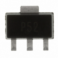
... Electronic hook switches • High Voltage Power MOSFET Drivers • Telecom call routers • Solid state relays ORDERING INFORMATION DEVICE REEL SIZE TAPE WIDTH (mm) (inches) ZVP4525ZTA 7 12mm embossed ZVP4525ZTC 13 12mm embossed DEVICE MARKING • P52 ISSUE 2 - JUNE 2007 ZVP4525Z D Top View ...
Page 2
ZVP4525Z ABSOLUTE MAXIMUM RATINGS PARAMETER Drain-Source Voltage Gate Source Voltage Continuous Drain Current (V GS =10V; TA=25°C)( =10V; TA=70°C)(a) Pulsed Drain Current (c) Continuous Source Current (Body Diode) Pulsed Source Current (Body Diode) Power Dissipation ...
Page 3
R DS(on) Limit 100m DC 1s 100ms 10m 10ms Single Pulse T =25°C amb Collector-Emitter Voltage (V) CE Safe Operating Area 120 T =25°C amb 100 80 D=0 D=0.2 20 D=0.1 0 100µ ...
Page 4
ZVP4525Z ELECTRICAL CHARACTERISTICS (at T PARAMETER STATIC Drain-Source Breakdown Voltage Zero Gate Voltage Drain Current Gate-Body Leakage Gate-Source Threshold Voltage Static Drain-Source On-State Resistance (1) Forward Transconductance (3) DYNAMIC (3) Input Capacitance Output Capacitance Reverse Transfer Capacitance SWITCHING(2) (3) Turn-On ...
Page 5
TYPICAL CHARACTERISTICS T = 25°C 1.0 0.8 0.6 0.4 0.2 0 Drain-Source Voltage (V) DS Output Characteristics 25°C 0 Gate-Source Voltage (V) GS Typical Transfer Characteristics 100 2V 2.5V 10 0.01 ...
Page 6
ZVP4525Z 175 C 150 125 100 0 Drain - Source Voltage (V) DS Capacitance v Drain-Source Voltage CHARACTERISTICS 10 ...
Page 7
ISSUE 2 - JUNE 2007 TEST CIRCUITS ZVP4525Z ...
Page 8
ZVP4525Z Definitions Product change Zetex Semiconductors reserves the right to alter, without notice, specifications, design, price or conditions of supply of any product or service. Customers are solely responsible for obtaining the latest relevant information before placing orders. Applications disclaimer ...
Page 9
PACKAGE DIMENSIONS DIM Millimetres Min Max Min A 4.40 4.60 0.173 B 3.75 4.25 0.150 C 1.40 1.60 0.550 0.28 0.45 0.011 G 0.38 0.55 0.015 H 1.50 1.80 0.060 K 2.60 2.85 0.102 L ...