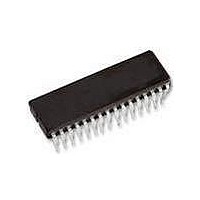
TDA8933T NXP Semiconductors, TDA8933T Datasheet - Page 29

TDA8933T
Manufacturer Part Number
TDA8933T
Description
Audio Amplifiers 2X10W BTL CLASS D AMP+VOLCTRL
Manufacturer
NXP Semiconductors
Datasheet
1.TDA8933TN1112.pdf
(47 pages)
Specifications of TDA8933T
Product
Class-D
Output Power
32 W
Available Set Gain
36 dB
Common Mode Rejection Ratio (min)
75 dB
Thd Plus Noise
0.011 %
Operating Supply Voltage
25 V
Supply Current
0.6 mA
Maximum Power Dissipation
5000 mW
Maximum Operating Temperature
+ 85 C
Mounting Style
SMD/SMT
Audio Load Resistance
16 Ohms
Dual Supply Voltage
+/- 12.5 V
Input Signal Type
Differential
Minimum Operating Temperature
- 40 C
Output Signal Type
Differential, Single
Supply Type
Single or Dual
Supply Voltage (max)
36 V
Supply Voltage (min)
10 V
Output Type
1-Channel Mono or 2-Channel Stereo
Package / Case
SOIC-32
Lead Free Status / RoHS Status
Lead free / RoHS Compliant
Other names
TDA8933T/N1,112
Available stocks
Company
Part Number
Manufacturer
Quantity
Price
Part Number:
TDA8933T
Manufacturer:
NXP/恩智浦
Quantity:
20 000
Company:
Part Number:
TDA8933T/N1
Manufacturer:
AMC
Quantity:
475
Part Number:
TDA8933T/N1
Manufacturer:
NXP/恩智浦
Quantity:
20 000
Part Number:
TDA8933T/N1,118
Manufacturer:
NXP/恩智浦
Quantity:
20 000
NXP Semiconductors
TDA8933_1
Preliminary data sheet
14.7 Thermal behavior (printed-circuit board considerations)
14.8 Pumping effects
R
The heat sink in an application with a TDA8933 is made using the copper on the
printed-circuit board. The TDA8933 uses the four corner leads (pins 1, 16, 17 and 32) for
heat transfer from the die to the PCB. The thermal foldback will limit the maximum junction
temperature to 140 C.
Equation 10
the thermal resistance from junction to ambient.
Where:
The power dissipation is shown in
The thermal resistance, R
copper, FR4 base material in free air with natural convection, is 44 K/W (typ.).
When the amplifier is used in an SE configuration, a so-called ‘pumping effect’ can occur.
During one switching interval, energy is taken from one supply (e.g. V
that energy is delivered back to the other supply line (e.g. V
the power supply cannot sink energy, the voltage across the output capacitors of that
power supply will increase.
The voltage increase caused by the pumping effect depends on:
The pumping effect should not cause a malfunction of either the audio amplifier or the
power supply. For instance, this malfunction can be caused by triggering of the
undervoltage or overvoltage protection of the amplifier.
Pumping effects in an SE configuration can be minimized by connecting audio inputs in
anti-phase and changing the polarity of one speaker, as shown in
th j a
•
•
•
•
•
R
T
T
P = power dissipation (W), which is determined by the efficiency of the TDA8933
j(max)
amb
th(j-a)
Speaker impedance
Supply voltage
Audio signal frequency
Value of decoupling capacitors on supply lines
Source and sink currents of other channels
–
= ambient temperature ( C)
=
= thermal resistance from junction to ambient (K/W)
= maximum junction temperature ( C)
T
----------------------------------- -
shows the relation between the maximum allowable power dissipation P and
j max
P
–
T
amb
Rev. 01 — 15 May 2007
th(j-a)
, of a 2 layer application board (55 mm
Figure 21
(SE) and
Figure 33
SSP1
), and vice versa. When
Class-D audio amplifier
(BTL).
Figure
DDP1
TDA8933
© NXP B.V. 2007. All rights reserved.
45 mm), 35 m
11.
), while a part of
29 of 47
(10)


