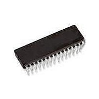
TDA8933T NXP Semiconductors, TDA8933T Datasheet - Page 7

TDA8933T
Manufacturer Part Number
TDA8933T
Description
Audio Amplifiers 2X10W BTL CLASS D AMP+VOLCTRL
Manufacturer
NXP Semiconductors
Datasheet
1.TDA8933TN1112.pdf
(47 pages)
Specifications of TDA8933T
Product
Class-D
Output Power
32 W
Available Set Gain
36 dB
Common Mode Rejection Ratio (min)
75 dB
Thd Plus Noise
0.011 %
Operating Supply Voltage
25 V
Supply Current
0.6 mA
Maximum Power Dissipation
5000 mW
Maximum Operating Temperature
+ 85 C
Mounting Style
SMD/SMT
Audio Load Resistance
16 Ohms
Dual Supply Voltage
+/- 12.5 V
Input Signal Type
Differential
Minimum Operating Temperature
- 40 C
Output Signal Type
Differential, Single
Supply Type
Single or Dual
Supply Voltage (max)
36 V
Supply Voltage (min)
10 V
Output Type
1-Channel Mono or 2-Channel Stereo
Package / Case
SOIC-32
Lead Free Status / RoHS Status
Lead free / RoHS Compliant
Other names
TDA8933T/N1,112
Available stocks
Company
Part Number
Manufacturer
Quantity
Price
Part Number:
TDA8933T
Manufacturer:
NXP/恩智浦
Quantity:
20 000
Company:
Part Number:
TDA8933T/N1
Manufacturer:
AMC
Quantity:
475
Part Number:
TDA8933T/N1
Manufacturer:
NXP/恩智浦
Quantity:
20 000
Part Number:
TDA8933T/N1,118
Manufacturer:
NXP/恩智浦
Quantity:
20 000
NXP Semiconductors
TDA8933_1
Preliminary data sheet
8.2 Mode selection and interfacing
The TDA8933 can be switched to one of four operating modes using pins POWERUP and
ENGAGE:
Both pins POWERUP and ENGAGE refer to pin CGND.
Table 4
ENGAGE pins.
Table 4.
[1]
If the transition between Mute mode and Operating mode is controlled via a time constant,
the start-up will be pop free since the DC output offset voltage is applied gradually to the
output between Mute mode and Operating mode. The bias current setting of the
V
The time constant required to apply the DC output offset voltage gradually between Mute
mode and Operating mode can be generated by applying a decoupling capacitor on pin
ENGAGE. The value of the capacitor on pin ENGAGE should be 470 nF.
Mode
Sleep
Mute
Operating
Fault
•
•
•
•
I
•
•
-converters is related to the voltage on pin ENGAGE.
Sleep mode: with low supply current
Mute mode: the amplifiers are switching idle (50 % duty cycle), but the audio signal at
the output is suppressed by disabling the V
pins HVP1 and HVP2 have been charged to half the supply voltage (asymmetrical
supply only)
Operating mode: the amplifiers are fully operational with an output signal
Fault mode
When there are symmetrical supply conditions, the voltage applied to pins POWERUP and ENGAGE must
never exceed the supply voltage (V
Mute mode: the bias current setting of the V
disabled).
Operating mode: the bias current is at maximum.
shows the different modes as a function of the voltages on the POWERUP and
Mode selection for the TDA8933
Pin
POWERUP
< 0.8 V
2 V to 6 V
2 V to 6 V
2 V to 6 V
Rev. 01 — 15 May 2007
DDA
[1]
, V
DDP1
or V
DDP2
ENGAGE
< 0.8 V
< 0.8 V
3 V to 6 V
undefined
l
-converter input stages. The capacitors on
I
).
-converters is zero (V
[1]
Class-D audio amplifier
DIAG
undefined
> 2 V
> 2 V
< 0.8 V
I
TDA8933
-converters
© NXP B.V. 2007. All rights reserved.
7 of 47


