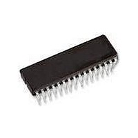
TDA8933T NXP Semiconductors, TDA8933T Datasheet - Page 8

TDA8933T
Manufacturer Part Number
TDA8933T
Description
Audio Amplifiers 2X10W BTL CLASS D AMP+VOLCTRL
Manufacturer
NXP Semiconductors
Datasheet
1.TDA8933TN1112.pdf
(47 pages)
Specifications of TDA8933T
Product
Class-D
Output Power
32 W
Available Set Gain
36 dB
Common Mode Rejection Ratio (min)
75 dB
Thd Plus Noise
0.011 %
Operating Supply Voltage
25 V
Supply Current
0.6 mA
Maximum Power Dissipation
5000 mW
Maximum Operating Temperature
+ 85 C
Mounting Style
SMD/SMT
Audio Load Resistance
16 Ohms
Dual Supply Voltage
+/- 12.5 V
Input Signal Type
Differential
Minimum Operating Temperature
- 40 C
Output Signal Type
Differential, Single
Supply Type
Single or Dual
Supply Voltage (max)
36 V
Supply Voltage (min)
10 V
Output Type
1-Channel Mono or 2-Channel Stereo
Package / Case
SOIC-32
Lead Free Status / RoHS Status
Lead free / RoHS Compliant
Other names
TDA8933T/N1,112
Available stocks
Company
Part Number
Manufacturer
Quantity
Price
Part Number:
TDA8933T
Manufacturer:
NXP/恩智浦
Quantity:
20 000
Company:
Part Number:
TDA8933T/N1
Manufacturer:
AMC
Quantity:
475
Part Number:
TDA8933T/N1
Manufacturer:
NXP/恩智浦
Quantity:
20 000
Part Number:
TDA8933T/N1,118
Manufacturer:
NXP/恩智浦
Quantity:
20 000
NXP Semiconductors
TDA8933_1
Preliminary data sheet
Fig 3. Start-up sequence
OUT1, OUT2
HVP1, HVP2
POWERUP
ENGAGE
HVPREF
OSCIO
DREF
8.3 Pulse width modulation frequency
audio
PWM
DIAG
V
P
0.43V
0.3V
The output signal of the amplifier is a PWM signal with a carrier frequency of
approximately 320 kHz. Using a 2nd-order-low-pass filter in the application results in an
analog audio signal across the loudspeaker. The PWM switching frequency can be set by
an external resistor R
frequency can be set between 300 kHz and 500 kHz. Using an external resistor of 39 k ,
the carrier frequency is set to an optimized value of 320 kHz (see
If two or more TDA8933 devices are used in the same audio application, it is
recommended to synchronize the switching frequency of all devices.This can be done by
connecting all the OSCIO pins together and configuring one of the TDA8933 devices in
the application as the clock master. Configure the other TDA8933 devices as slaves.
Pin OSCIO is a 3-state input or output buffer. Pin OSCIO is configured in master mode as
oscillator output, and in slave mode as oscillator input. Master mode is enabled by
applying a resistor between pin OSCREF and V
connecting pin OSCREF directly to V
The value of the resistor also sets the frequency of the carrier and can be calculated with
Equation
ENGAGE
ENGAGE
1:
operating
AUDIO
osc
Rev. 01 — 15 May 2007
connected between pin OSCREF and V
PWM
mute
operating
AUDIO
SSD(HW)
fault
(without any resistor).
SSD(HW)
, while slave mode is enabled by
operating
AUDIO
PWM
Class-D audio amplifier
SSD(HW)
Figure
0.17V
TDA8933
© NXP B.V. 2007. All rights reserved.
001aae788
ENGAGE
. The carrier
4).
sleep
8 of 47


