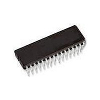
TDA8932T NXP Semiconductors, TDA8932T Datasheet - Page 7

TDA8932T
Manufacturer Part Number
TDA8932T
Description
Audio Amplifiers 2X15W BTL CLASS D AMP+VOLCTRL
Manufacturer
NXP Semiconductors
Datasheet
1.TDA8932TN1112.pdf
(45 pages)
Specifications of TDA8932T
Product
Class-D
Output Power
50 W
Available Set Gain
36 dB
Common Mode Rejection Ratio (min)
56 dB
Thd Plus Noise
0.015 %
Operating Supply Voltage
22 V
Maximum Power Dissipation
5000 mW
Maximum Operating Temperature
+ 85 C
Mounting Style
SMD/SMT
Audio Load Resistance
8 Ohms
Dual Supply Voltage
+/- 11 V
Input Signal Type
Differential
Minimum Operating Temperature
- 40 C
Output Signal Type
Differential, Single
Supply Type
Single or Dual
Supply Voltage (max)
36 V
Supply Voltage (min)
10 V
Output Type
1-Channel Mono or 2-Channel Stereo
Package / Case
SOIC-32
Lead Free Status / RoHS Status
Lead free / RoHS Compliant
Other names
TDA8932T/N1,112
Available stocks
Company
Part Number
Manufacturer
Quantity
Price
Company:
Part Number:
TDA8932T
Manufacturer:
PHILIPS
Quantity:
9
Part Number:
TDA8932T
Manufacturer:
NXP/恩智浦
Quantity:
20 000
Company:
Part Number:
TDA8932T/N1
Manufacturer:
EPSON
Quantity:
6
Part Number:
TDA8932T/N1
Manufacturer:
NXP/恩智浦
Quantity:
20 000
Part Number:
TDA8932T/N1,118
Manufacturer:
NXP/恩智浦
Quantity:
20 000
Part Number:
TDA8932T/N1.518
Manufacturer:
NXP/恩智浦
Quantity:
20 000
NXP Semiconductors
TDA8932_2
Preliminary data sheet
Fig 3. Start-up sequence
OUT1, OUT2
HVP1, HVP2
POWERUP
ENGAGE
HVPREF
OSCIO
DREF
8.3 Pulse width modulation frequency
audio
PWM
DIAG
V
P
0.43V
0.3V
If the transition between Mute mode and Operating mode is controlled via a time constant,
the start-up will be pop free since the DC output offset voltage is applied gradually to the
output between Mute mode and Operating mode. The bias current setting of the
VI-converters is related to the voltage on pin ENGAGE:
The time constant required to apply the DC output offset voltage gradually between Mute
mode and Operating mode can be generated by applying a decoupling capacitor on pin
ENGAGE. The value of the capacitor on pin ENGAGE should be 470 nF.
The output signal of the amplifier is a PWM signal with a carrier frequency of
approximately 320 kHz. Using a 2nd-order low-pass filter in the application results in an
analog audio signal across the loudspeaker. The PWM switching frequency can be set by
an external resistor R
frequency can be set between 300 kHz and 500 kHz. Using an external resistor of 39 k ,
the carrier frequency is set to an optimized value of 320 kHz (see
•
•
ENGAGE
ENGAGE
Mute mode: the bias current setting of the VI-converters is zero (VI-converters
disabled)
Operating mode: the bias current is at maximum
operating
AUDIO
Rev. 02 — 12 December 2006
osc
connected between pins OSCREF and V
PWM
mute
operating
AUDIO
fault
operating
AUDIO
PWM
Class-D audio amplifier
Figure
SSD(HW)
0.17V
TDA8932
© NXP B.V. 2006. All rights reserved.
001aae788
ENGAGE
4).
. The carrier
sleep
7 of 45


