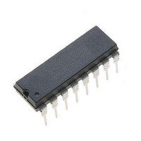
ML2021CP Fairchild Semiconductor, ML2021CP Datasheet - Page 8

ML2021CP
Manufacturer Part Number
ML2021CP
Description
Telecom Voice Conditioning ICs Phone Line Equalizer Group Delay Tuned
Manufacturer
Fairchild Semiconductor
Datasheet
1.ML2021CP.pdf
(11 pages)
Specifications of ML2021CP
Mounting Style
Through Hole
Package / Case
DIP-16
Lead Free Status / RoHS Status
Lead free / RoHS Compliant
Available stocks
Company
Part Number
Manufacturer
Quantity
Price
Company:
Part Number:
ML2021CP
Manufacturer:
FAR
Quantity:
5 510
Company:
Part Number:
ML2021CP
Manufacturer:
NEC
Quantity:
5 510
ML2021
Table 3. Slope Response Factors (b,c)
Table 4. Slope Response factors (b,c)
Table 5. Height Response Factors (h)
8
S3-0
0000
0001
0010
0011
0100
0101
0110
0111
1000
1001
1010
1011
1100
1101
1110
1111
S3-0
XXXX
B3-0
0000
0001
0010
0011
0100
0101
0110
0111
1000
1001
1010
1011
1100
1101
1110
1111
Code
0000
0001
0010
0011
0100
0101
0110
0111
1000
1001
1010
1011
1100
1101
1110
1111
b
NL/L = 0
2.371759E +03
1.985920E + 03
1.701779E + 03
1.493571E + 03
1.326721E + 03
1.196668E + 03
1.087277E + 03
9.983588E + 02
9.179889E + 02
8.537864E + 02
7.966049E + 02
7.478074E + 02
7.035099E + 02
6.651771E + 02
6.299477E + 02
5.990361E + 02
c
NL/L = 0
2.371759E + 03
Q
17.444906
15.386148
13.652451
11.593677
9.859960
8.017864
6.392453
5.092080
3.900003
3.141338
2.599369
2.165724
1.731965
1.406509
1.352248
1.297981
h
1.000000
1.071519
1.148154
1.230269
1.318257
1.445438
1.603245
1.757924
1.949845
2.137962
2.317395
2.540973
2.786121
3.019951
3.311311
3.672823
b
NL/L = 1
1.116280E + 04
9.345141E + 03
8.007156E + 03
7.026999E + 03
6.241681E + 03
5.629636E + 03
5.114881E + 03
4.696487E + 03
4.318339E + 03
4.016273E + 03
3.747249E + 03
3.517676E + 03
3.309279E + 03
3.128945E + 03
2.963214E + 03
2.817797E + 03
c
NL/L = 1
1.116280E + 04
Group Delay
The difference between the ML2020 and ML2021 is the
elimination of a 60 Hz highpass filter in order to eliminate
positive group delay at low frequency.
The group delay through the ML2021 can be minimized
such that less than 50µs of group delay can be achieved
in both unloaded and cable loaded conditions relative to
1804 Hz in the frequency range of 504 to 3004Hz. Minimum
group delays are dependant upon using the proper
setting for slope, height, and bandwidth for a give equaliza-
tion requirement.
Smoothing Filter
The equalizer filters are followed by a continuous second
order smoothing filter that removes the high frequency
sample information generated by the action of the switched
capacitor filters. This filter provides a continuous analog
signal at the output, V
Output Buffer
The final stage in the ML2021 is the output buffer. This
amplifier has internal gain of 1 and is capable of driving
600Ω, 100pF loads. Thus, it is suitable for driving telephone
hybrids directly without any external amplifier.
Bypass Mode
The filter sections can be bypassed by setting the bypass data
bit, BP, to 0. Since the switched capacitor filters are bypassed
in this mode, frequency response effects of the switched
capacitor filters are eliminated. Thus, this mode offers very
flat response and low noise over the 300-4000 Hz frequency
range.
Filter Clock
The master clock, CLK, is used to generate the internal
clocks for the switched capacitor filters. The frequency of
CLK can be either 1.544 MHz or 1.536 MHz. However, the
internal clock frequency must be kept at 1.536 MHz to
guarantee accurate frequency response. The CLKSEL pin
enables a bit swallower circuit to keep the internal clock
frequency set to 1.536 MHz. When 1.544 MHz clock is used,
CLKSEL should be set to logic level 0, and one bit out of
every 193 bits is removed (swallowed) to reduce the internal
frequency to 1.536 MHz. When 1.536 MHz clock is used,
CLKSEL should be set to logic level 1, and the internal clock
rate is the same as the external clock rate.
Serial Interface
The architecture of the digital section is shown in the preced-
ing block diagram.
A timing diagram for the serial interface is shown in Figure
6. The serial input data, SID, is loaded into a shift register on
rising edges of the shift clock, SCK. The data word is paral-
lel loaded into a latch when the input latch signal, LATI, is
OUT
.
PRODUCT SPECIFICATION
REV. 1.1.1 3/19/01


