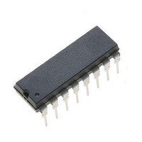
ML2021IP Fairchild Semiconductor, ML2021IP Datasheet - Page 2

ML2021IP
Manufacturer Part Number
ML2021IP
Description
Telecom Voice Conditioning ICs Phone Line Equalizer Group Delay Tuned
Manufacturer
Fairchild Semiconductor
Datasheet
1.ML2021IP.pdf
(11 pages)
Specifications of ML2021IP
Mounting Style
Through Hole
Package / Case
DIP-16
Lead Free Status / RoHS Status
Lead free / RoHS Compliant
Available stocks
Company
Part Number
Manufacturer
Quantity
Price
Company:
Part Number:
ML2021IP
Manufacturer:
ALCATEL
Quantity:
6 218
ML2021
Pin Description
Absolute Maximum Ratings
Operating Conditions
2
Name
CLKSEL
SID
LATO
SCK
SOD
CLK
GND
LATI
V
V
AGND
V
P
V
Parameter
Supply Voltage
AGND with respect to GND
Analog Input and Output
Digital Input and Outputs
Input Current Per Pin
Power Dissipation
Storage Temperature Range
Lead Temperature (Soldering, 10 sec)
Parameter
Temperature Range
Supply Voltage
SS
IN
OUT
DN
CC
V
V
ML2021CX
ML2021IX
V
V
CC
SS
CC
SS
Clock select input. This pin selects the frequency of the CLK input. If CLK is 1.536 MHz, set
CLKSEL = 1. If CLK is 1.544 MHz, set CLKSEL = 0. Pin has an internal pullup resistor to V
Serial input data. Digital input that contains serial data word which controls the filter frequency
response setting.
Output latch clock. Digital input which loads the data word back into the shift register from the latch.
Shift clock. Digital input which shifts the serial data on SID into the shift register on rising edges and
out onto SOD on falling edges.
Serial output data. Digital output of the shift register.
Master clock input. Digital input which generates clocks for the switched capacitor filters.
Frequency can be either 1.544 MHz or 1.536 MHz.
Digital ground. 0 volts. All digital inputs and output are referenced to this ground.
Input latch clock. Digital input which loads data from the shift register into the latch.
Negative supply. –5volts ±10%.
Analog input.
Analog ground. 0 volts. Analog input and output are referenced to this ground.
Analog output.
Powerdown input. When P
operation. This pin has an internal pulldown resistor to GND.
Positive supply. 5 volts ± 10%
2
DN
1
= 1, device is in powerdown mode. When P
Function
GND –0.3
V
SS
Min.
Min.
-40
-65
-4
0
4
–0.3
ND
V
V
CC
CC
Max.
Max.
+150
+6.5
±0.5
PRODUCT SPECIFICATION
-6.5
±25
750
300
= 0, device is in normal
70
85
-6
6
+0.3
+0.3
REV. 1.1.1 3/19/01
CC
Units
Units
mW
mA
°C
°C
°C
°C
.
V
V
V
V
V
V
V


