FDMS2572 Fairchild Semiconductor, FDMS2572 Datasheet
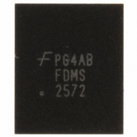
MOSFET N-CH 150V 4.5A POWER56

FDMS2572

Manufacturer Part Number
FDMS2572
Description
MOSFET N-CH 150V 4.5A POWER56
Manufacturer
Fairchild Semiconductor
Series
UltraFET™r
Datasheet

Specifications of FDMS2572

Fet Type
MOSFET N-Channel, Metal Oxide
Fet Feature
Logic Level Gate
Rds On (max) @ Id, Vgs
47 mOhm @ 4.5A, 10V
Drain To Source Voltage (vdss)
150V
Current - Continuous Drain (id) @ 25° C
4.5A
Vgs(th) (max) @ Id
4V @ 250µA
Gate Charge (qg) @ Vgs
43nC @ 10V
Input Capacitance (ciss) @ Vds
2610pF @ 75V
Power - Max
2.5W
Mounting Type
Surface Mount
Package / Case
8-MLP, Power56
Configuration
Single Quad Drain Triple Source
Transistor Polarity
N-Channel
Resistance Drain-source Rds (on)
0.036 Ohms
Forward Transconductance Gfs (max / Min)
14 S
Drain-source Breakdown Voltage
150 V
Gate-source Breakdown Voltage
+/- 20 V
Continuous Drain Current
4.5 A
Power Dissipation
2.5 W
Maximum Operating Temperature
+ 150 C
Mounting Style
SMD/SMT
Minimum Operating Temperature
- 55 C
Lead Free Status / RoHS Status
Lead free / RoHS Compliant
Other names
FDMS2572TR

Available stocks

Company
Part Number
Manufacturer
Quantity
Price
Part Number:
FDMS2572
Manufacturer:
Fairchild Semiconductor
Quantity:
57 589
Part Number:
FDMS2572
Manufacturer:
FAIRCHILD/仙童
Quantity:
20 000
Part Number:
FDMS2572
Quantity:
2 084
Company:
Part Number:
FDMS2572
Quantity:
5 000
©2007 Fairchild Semiconductor Corporation
FDMS2572 Rev.C2
FDMS2572
N-Channel UltraFET Trench
150V, 27A, 47mΩ
Features
MOSFET Maximum Ratings
Thermal Characteristics
Package Marking and Ordering Information
V
V
I
P
T
R
R
D
DS
GS
D
J
θJC
θJA
Max r
Max r
Low Miller Charge
Optimized efficiency at high frequencies
UIS Capability (Single pulse and Repetitive pulse)
RoHS Compliant
, T
Symbol
Device Marking
STG
FDMS2572
DS(on)
DS(on)
Pin 1
= 47mΩ at V
= 53mΩ at V
Drain to Source Voltage
Gate to Source Voltage
Drain Current -Continuous (Package limited)
Power Dissipation
Power Dissipation
Operating and Storage Junction Temperature Range
Thermal Resistance, Junction to Case
Thermal Resistance, Junction to Ambient
Power 56 (Bottom view)
D
GS
GS
S
D
= 10V, I
= 6V, I
FDMS2572
-Continuous
-Continuous (Silicon limited)
-Pulsed
S
Device
D
D
D
S
D
= 4.5A
= 4.5A
G
T
A
= 25°C unless otherwise noted
Parameter
Power 56
Package
®
1
MOSFET
T
T
T
T
T
C
General Description
UItraFET
benchmark efficiency in power conversion applications.
Optimized for r
these devices are ideal for high frequency DC to DC converters.
Application
C
C
A
D
D
D
D
A
= 25°C
= 25°C
= 25°C
= 25°C
= 25°C
Distributed Power Architectures and VRMs
Primary Switch for 24V and 48V Systems
High Voltage Synchronous Rectifier
5
6
7
8
Reel Size
devices
13’’
DS(on)
(Note 1a)
(Note 1a)
(Note 1a)
, low ESR, low total and Miller gate charge,
combine
Tape Width
12mm
characteristics
4
3
2
1
-55 to +150
Ratings
S
S
G
S
150
±20
4.5
2.5
1.6
27
27
30
78
50
February 2007
www.fairchildsemi.com
3000 units
that
Quantity
Units
°C/W
enable
°C
W
V
V
A
tm

Related parts for FDMS2572

FDMS2572 Summary of contents

Page 1

... Thermal Resistance, Junction to Case θJC R Thermal Resistance, Junction to Ambient θJA Package Marking and Ordering Information Device Marking Device FDMS2572 FDMS2572 ©2007 Fairchild Semiconductor Corporation FDMS2572 Rev.C2 ® MOSFET General Description = 4.5A UItraFET D benchmark efficiency in power conversion applications. = 4.5A D Optimized for r these devices are ideal for high frequency converters. ...

Page 2

... Reverse Recovery Time rr Q Reverse Recovery Charge rr Notes determined with the device mounted on a 1in θJA the user's board design. 2: Pulse Test: Pulse Width < 300µs, Duty cycle < 2.0%. FDMS2572 Rev. 25°C unless otherwise noted J Test Conditions I = 250µ 250µA, referenced to 25°C ...

Page 3

... T , JUNCTION TEMPERATURE J Figure 3. Normalized On - Resistance vs Junction Temperature 60 PULSE DURATION = 300 DUTY CYCLE = 2.0%MAX GATE TO SOURCE VOLTAGE (V) GS Figure 5. Transfer Characteristics FDMS2572 Rev. 25°C unless otherwise noted J µ 4. 100 125 150 µ 125 1E =-55 C ...

Page 4

... TIME IN AVALANCHE(ms) AV Figure 9. Unclamped Inductive Switching Capability 0.1 OPERATION IN THIS AREA MAY BE LIMITED BY r 0.01 DS(on) SINGLE PULSE MAX RATED 1E-3 0 DRAIN to SOURCE VOLTAGE (V) Figure 11. Forward Bias Safe Operating Area FDMS2572 Rev. 25°C unless otherwise noted J 3000 =50V 1000 V = 75V 100V DD 100 ...

Page 5

... Typical Characteristics 2 1 DUTY CYCLE-DESCENDING ORDER D = 0.5 0.2 0.1 0.1 0.05 0.02 0.01 0.01 SINGLE PULSE 1E-3 5E FDMS2572 Rev. 25°C unless otherwise noted RECTANGULAR PULSE DURATION (s) Figure 13. Transient Thermal Response Curve NOTES: DUTY FACTOR PEAK θJA θ www.fairchildsemi.com ...

Page 6

... FDMS2572 Rev.C2 6 www.fairchildsemi.com ...

Page 7

... PRODUCT STATUS DEFINITIONS Definition of Terms Datasheet Identification Advance Information Preliminary No Identification Needed Obsolete FDMS2572 Rev. C2 OCX™ SILENT SWITCHER OCXPro™ SMART START™ ® OPTOLOGIC SPM™ OPTOPLANAR™ ...

Related keywords