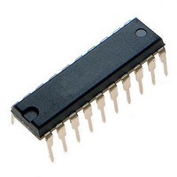
ETC5067N/C STMicroelectronics, ETC5067N/C Datasheet

ETC5067N/C
Specifications of ETC5067N/C
Available stocks
Related parts for ETC5067N/C
ETC5067N/C Summary of contents
Page 1
SERIAL INTERFACE CODEC/FILTER WITH RECEIVE . COMPLETE CODEC AND FILTERING SYS- TEM INCLUDING : - Transmit high-pass and low-pass filtering. - Receive low-pass filter with sin x/x correction. - Active RC noise filter. - -law or A-law compatible CODER ...
Page 2
ETC5064 - ETC5064-X - ETC5067 - ETC5067-X PIN CONNECTIONS (Top views) DIP20 & SO20 BLOCK DIAGRAM (ETC5064 - ETC5064-X - ETC5067 - ETC5067-X) 2/18 PLCC20 ...
Page 3
PIN DESCRIPTION Pin Name Type (*) + VPO O GNDA GND - VPO O VPI BCLK /CLKSEL I R MCKL /PDN I R MCLK I X ...
Page 4
ETC5064 - ETC5064-X - ETC5067 - ETC5067-X FUNCTIONAL DESCRIPTION POWER-UP When power is first applied, power-on reset circuitry initializes the device and places it into the power- down mode. All non-essential circuits are deacti- vated and the D and VF ...
Page 5
For 64 kHz operation, the frame sync pulses must be kept low for a minimum of 160 ns (see Fig 1). The D X buffer is enabled with the rising edge of FS rising edge of ...
Page 6
ETC5064 - ETC5064-X - ETC5067 - ETC5067-X ELECTRICAL OPERATING CHARACTERISTICS V = 5.0V 5 -5V 5%, GNDA = 0V otherwise noted; typical characteristics specified at V enced to GNDA. DIGITAL INTERFACE (All devices) Symbol V ...
Page 7
ELECTRICAL OPERATING CHARACTERISTICS (Continued) ANALOG INTERFACE WITH POWER AMPLIFIERS (all devices) Symbol IPI Input Leakage Current (– 1.0 V RIPI Input Resistance (– 1.0 VIOS Input Offset Voltage ROP Output Resistance (inverting unity–gain at VPO F Unity–gain Bandwidth, Open Loop ...
Page 8
ETC5064 - ETC5064-X - ETC5067 - ETC5067-X All TIMING SPECIFICATIONS Symbol 1/t Frequency of master clocks PM MCLK and MCLK X Depends on the device used and the BCLK /CLKSEL Pin R t Width of Master Clock High WMH t ...
Page 9
Figure 2 : Short Frame Sync Timing. ETC5064 - ETC5064-X - ETC5067 - ETC5067-X 9/18 ...
Page 10
ETC5064 - ETC5064-X - ETC5067 - ETC5067-X Figure 3 : Long Frame Sync Timing. 10/18 ...
Page 11
TRANSMISSION CHARACTERISTICS (all devices 0°C to 70°C (ETC5064-X/67- GNDA = 0V 1.02kHz 0dBm0 transmit input amplifier connected for unity–gain non–inverting. (unless IN otherwise specified). AMPLITUDE RESPONSE Symbol Absolute Levels - Nominal 0 ...
Page 12
ETC5064 - ETC5064-X - ETC5067 - ETC5067-X TRANSMISSION CHARACTERISTICS (continued). ENVELOPE DELAY DISTORTION WITH FREQUENCY Symbol D Transmit Delay, Absolute (f = 1600 Hz Transmit Delay, Relative 500 Hz-600 600 ...
Page 13
TRANSMISSION CHARACTERISTICS (continued). DISTORTION Symbol STD Signal to Total Distortion (sinusoidal test method STD Transmit or Receive Half-channel R Level = 3.0 dBm0 = 0 dBm0 to – 30 dBm0 = – 40 dBm0 = – 55 dBm0 ...
Page 14
ETC5064 - ETC5064-X - ETC5067 - ETC5067-X APPLICATION INFORMATION POWER SUPPLIES While the pins at the ETC506X family are well pro- tected against electrical misure recommended that the standard CMOS practice be followed, en- suring that ground is ...
Page 15
DIM. MIN. TYP. MAX. MIN. A 2.35 2.65 0.093 A1 0.1 0.3 0.004 B 0.33 0.51 0.013 C 0.23 0.32 0.009 D 12.6 13 0.496 E 7.4 7.6 0.291 e 1. 10.65 0.394 h 0.25 0.75 0.010 ...
Page 16
ETC5064 - ETC5064-X - ETC5067 - ETC5067-X mm DIM. MIN. TYP. MAX. A 9.78 10.03 0.385 B 8.89 9.04 0.350 D 4.2 4.57 0.165 d1 2.54 d2 0.56 E 7.37 8.38 0.290 e 1.27 F 0.38 G 0.101 M 1.27 ...
Page 17
DIM. MIN. TYP. MAX. MIN. a1 0.254 0.010 B 1.39 1.65 0.055 b 0.45 b1 0.25 D 25.4 E 8.5 e 2.54 e3 22.86 F 7.1 I 3.93 L 3.3 Z 1.34 ETC5064 - ETC5064-X - ETC5067 - ETC5067-X ...
Page 18
... No license is granted by implication or otherwise under any patent or patent rights of STMicroelectronics. Specifications mentioned in this publication are subject to change without notice. This publication supersedes and replaces all information previously supplied. STMi- croelectronics products are not authorized for use as critical components in life support devices or systems without express written approval of STMicroelectronics ...


