FDPF33N25T Fairchild Semiconductor, FDPF33N25T Datasheet

MOSFET N-CH 250V 33A TO-220F

FDPF33N25T

Manufacturer Part Number
FDPF33N25T
Description
MOSFET N-CH 250V 33A TO-220F
Manufacturer
Fairchild Semiconductor
Series
UniFET™r
Datasheets

Specifications of FDPF33N25T

Fet Type
MOSFET N-Channel, Metal Oxide
Fet Feature
Standard
Rds On (max) @ Id, Vgs
94 mOhm @ 16.5A, 10V
Drain To Source Voltage (vdss)
250V
Current - Continuous Drain (id) @ 25° C
33A
Vgs(th) (max) @ Id
5V @ 250µA
Gate Charge (qg) @ Vgs
48nC @ 10V
Input Capacitance (ciss) @ Vds
2135pF @ 25V
Power - Max
37W
Mounting Type
Through Hole
Package / Case
TO-220-3 Full Pack (Straight Leads)
Transistor Polarity
N Channel
Continuous Drain Current Id
20A
Drain Source Voltage Vds
250V
On Resistance Rds(on)
94mohm
Rds(on) Test Voltage Vgs
10V
Threshold Voltage Vgs Typ
5V
Rohs Compliant
Yes
Configuration
Single
Resistance Drain-source Rds (on)
0.077 Ohms
Forward Transconductance Gfs (max / Min)
26.6 S
Drain-source Breakdown Voltage
250 V
Gate-source Breakdown Voltage
+/- 30 V
Continuous Drain Current
20 A
Power Dissipation
37 W
Maximum Operating Temperature
+ 150 C
Mounting Style
Through Hole
Minimum Operating Temperature
- 55 C
Lead Free Status / RoHS Status
Lead free / RoHS Compliant

Available stocks

Company
Part Number
Manufacturer
Quantity
Price
Part Number:
FDPF33N25T
Manufacturer:
FSC
Quantity:
12 000
Part Number:
FDPF33N25T
Manufacturer:
ON/安森美
Quantity:
20 000
Company:
Part Number:
FDPF33N25T
Quantity:
3 000
©2006 Fairchild Semiconductor Corporation
FDPF33N25 Rev A
FDPF33N25
250V N-Channel MOSFET
Features
• 20A, 250V, R
• Low gate charge ( typical 36.8 nC)
• Low C
• Fast switching
• 100% avalanche tested
• Improved dv/dt capability
Absolute Maximum Ratings
Thermal Characteristics
V
I
I
V
E
I
E
dv/dt
P
T
T
R
R
D
DM
AR
J,
L
DSS
GSS
AS
AR
D
Symbol
Symbol
θJC
θJA
T
STG
rss
( typical 39 pF)
DS(on)
Drain-Source Voltage
Drain Current
Drain Current
Gate-Source voltage
Single Pulsed Avalanche Energy
Avalanche Current
Repetitive Avalanche Energy
Peak Diode Recovery dv/dt
Power Dissipation
Maximum Lead Temperature for Soldering Purpose,
1/8” from Case for 5 Seconds
Thermal Resistance, Junction-to-Case
Thermal Resistance, Junction-to-Ambient
Operating and Storage Temperature Range
= 0.094Ω @V
G
D
S
GS
- Continuous (T
- Continuous (T
- Pulsed
(T
- Derate above 25°C
= 10 V
Parameter
Parameter
C
FDPF Series
TO-220F
= 25°C)
C
C
= 25°C)
= 100°C)
1
Description
These N-Channel enhancement mode power field effect
transistors are produced using Fairchild’s proprietary, planar
stripe, DMOS technology.
This advanced technology has been especially tailored to
minimize on-state resistance, provide superior switching
performance, and withstand high energy pulse in the avalanche
and commutation mode. These devices are well suited for high
efficient switched mode power supplies and active power factor
correction.
(Note 2)
(Note 1)
(Note 1)
(Note 3)
(Note 1)
G
Min.
FDPF33N25
--
--
-55 to +150
0.76
250
±30
918
300
9.4
4.5
20
12
80
20
94
S
D
Max.
1.32
62.5
UniFET
May 2006
www.fairchildsemi.com
Unit
W/°C
V/ns
Unit
mJ
mJ
°C/W
°C/W
°C
°C
W
V
A
A
A
V
A
TM

Related parts for FDPF33N25T

FDPF33N25T Summary of contents

Page 1

... Thermal Characteristics Symbol R Thermal Resistance, Junction-to-Case θJC R Thermal Resistance, Junction-to-Ambient θJA ©2006 Fairchild Semiconductor Corporation FDPF33N25 Rev A Description = 10 V These N-Channel enhancement mode power field effect GS transistors are produced using Fairchild’s proprietary, planar stripe, DMOS technology. This advanced technology has been especially tailored to ...

Page 2

Package Marking and Ordering Information Device Marking Device FDPF33N25 FDPF33N25 Electrical Characteristics Symbol Parameter Off Characteristics BV Drain-Source Breakdown Voltage DSS ΔBV Breakdown Voltage Temperature DSS ΔT / Coefficient J I Zero Gate Voltage Drain Current DSS I Gate-Body Leakage ...

Page 3

Typical Performance Characteristics Figure 1. On-Region Characteristics Top : 15.0 V 10.0 V 8.0 V 7.0 V 6.5 V 6.0 V Bottom : 5 Drain-Source ...

Page 4

Typical Performance Characteristics Figure 7. Breakdown Voltage Variation vs. Temperature 1.2 1.1 1.0 0.9 0.8 -100 - Junction Temperature [ J Figure 9. Maximum Safe Operating Area Operation in This Area DC is ...

Page 5

Unclamped Inductive Switching Test Circuit & Waveforms FDPF33N25 Rev A Gate Charge Test Circuit & Waveform Resistive Switching Test Circuit & Waveforms 5 www.fairchildsemi.com ...

Page 6

FDPF33N25 Rev A Peak Diode Recovery dv/dt Test Circuit & Waveforms 6 www.fairchildsemi.com ...

Page 7

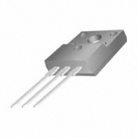
Mechanical Dimensions MAX1.47 0.80 ±0.10 0.35 ±0.10 2.54TYP [2.54 ] ±0.20 FDPF33N25 Rev A TO-220F 10.16 ø3.18 ±0.20 ±0.10 (7.00) (1.00x45°) #1 2.54TYP [2.54 ] ±0.20 9.40 ±0.20 7 2.54 ±0.20 (0.70) +0.10 0.50 2.76 ±0.20 –0.05 www.fairchildsemi.com ...

Page 8

... TRADEMARKS The following are registered and unregistered trademarks Fairchild Semiconductor owns or is authorized to use and is not intended exhaustive list of all such trademarks. ® ACEx™ FAST ActiveArray™ FASTr™ Bottomless™ FPS™ Build it Now™ FRFET™ CoolFET™ ...

Related keywords