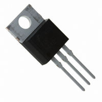
FDP8440 Fairchild Semiconductor, FDP8440 Datasheet - Page 2

FDP8440
Manufacturer Part Number
FDP8440
Description
MOSFET N-CH 40V 100A TO-220
Manufacturer
Fairchild Semiconductor
Series
PowerTrench®r
Datasheet
1.FDP8440.pdf
(8 pages)
Specifications of FDP8440
Fet Type
MOSFET N-Channel, Metal Oxide
Fet Feature
Logic Level Gate
Rds On (max) @ Id, Vgs
2.2 mOhm @ 80A, 10V
Drain To Source Voltage (vdss)
40V
Current - Continuous Drain (id) @ 25° C
100A
Vgs(th) (max) @ Id
3V @ 250µA
Gate Charge (qg) @ Vgs
450nC @ 10V
Input Capacitance (ciss) @ Vds
24740pF @ 25V
Power - Max
306W
Mounting Type
Through Hole
Package / Case
TO-220-3 (Straight Leads)
Configuration
Single
Transistor Polarity
N-Channel
Resistance Drain-source Rds (on)
0.0022 Ohm @ 10 V
Drain-source Breakdown Voltage
40 V
Gate-source Breakdown Voltage
+/- 20 V
Continuous Drain Current
277 A
Power Dissipation
306000 mW
Maximum Operating Temperature
+ 175 C
Mounting Style
Through Hole
Minimum Operating Temperature
- 55 C
Lead Free Status / RoHS Status
Lead free / RoHS Compliant
Available stocks
Company
Part Number
Manufacturer
Quantity
Price
Company:
Part Number:
FDP8440
Manufacturer:
FSC
Quantity:
1 000
Company:
Part Number:
FDP8440
Manufacturer:
FAIRCHILD
Quantity:
1 250
FDP8440 Rev. A6
Package Marking and Ordering Information
Electrical Characteristics
NOTES:
1: Pulse width limited by maximum junction temperature.
2: Starting T
Off Characteristics
BV
I
I
On Characteristics
V
R
Dynamic Characteristics
C
C
C
R
Q
Q
Q
Q
Q
Switching Characteristics
t
t
t
t
t
t
Drain-Source Diode Characteristics and Maximum Ratings
V
t
Q
Device Marking
Symbol
DSS
GSS
ON
d(on)
r
d(off)
f
OFF
rr
GS(th)
SD
DS(on)
iss
oss
rss
G
g(tot)
g(2)
gs
gs2
gd
RR
DSS
FDP8440
J
= 25°C, L = 1mH, I
Drain to Source Breakdown Voltage
Zero Gate Voltage Drain Current
Gate to Body Leakage Current
Gate to Source Threshold Voltage
Static Drain-Source On-Resistance
Input Capacitance
Output Capacitance
Reverse Transfer Capacitance
Gate Resistance
Total Gate Charge at 10V
Threshold Gate Charge
Gate to Source Gate Charge
Gate Charge Threshold to Plateau
Gate to Drain “Miller” Charge
Turn-On Time
Turn-On Delay Time
Rise Time
Turn-Off Delay Time
Fall Time
Turn-Off Time
Source to Drain Diode Voltage
Reverse Recovery Time
Reverse Recovery Charge
AS
= 58A, V
Parameter
FDP8440
Device
(V
GS
DD
= 10V)
= 36V, V
GS
T
C
= 10V.
= 25°C unless otherwise noted
Package
TO-220
V
V
V
V
V
V
V
V
T
V
f = 1.0MHz
V
V
V
V
V
I
I
I
I
SD
SD
SD
SD
C
GS
DS
GS
GS
DS
GS
GS
GS
DS
GS
GS
GS
DD
GS
= 175
= 80A
= 40A
= 75A, dI
= 75A, dI
= 0V
= 32V
= V
= 25V, V
= 0V, I
= ±20V
= 4.5V, I
= 10V, I
= 10V, I
= 0.5V, f = 1MHz
= 0V to 10V
= 0V to 2V
= 20V,I
= 10V, R
GS
o
C
2
, I
D
Conditions
D
D
D
D
SD
SD
= 250μA
D
GS
GEN
= 80A
= 80A
= 80A,
= 250μA
= 80A
/dt = 100A/μs
/dt = 100A/μs
Reel Size
= 0V,
= 7Ω
N/A
T
V
I
I
D
g
C
DD
= 1.0mA
= 80A
= 150
= 20V
o
C
Tape Width
Min
N/A
40
--
--
--
--
--
--
--
--
--
--
--
--
--
--
--
--
--
--
--
--
--
--
--
--
--
1
18600
1840
1400
Typ
1.88
1.64
3.00
32.5
16.5
345
175
130
435
290
730
1.1
49
74
43
59
77
--
--
--
--
--
--
--
24740
Max
Quantity
±100
2450
2100
1470
1.25
250
450
360
275
875
590
2.4
2.2
4.4
1.0
95
www.fairchildsemi.com
--
--
--
--
--
--
--
--
1
3
50units
Units
mΩ
μA
μA
nA
nC
nC
nC
nC
nC
nC
pF
pF
pF
ns
ns
ns
ns
ns
ns
ns
Ω
V
V
V
V


