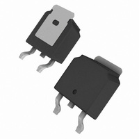
IRFPS37N50APBF Vishay, IRFPS37N50APBF Datasheet

IRFPS37N50APBF
Specifications of IRFPS37N50APBF
Available stocks
Related parts for IRFPS37N50APBF
IRFPS37N50APBF Summary of contents
Page 1
... Notes through … are on page 8 Document Number: 91258 SMPS MOSFET V DSS 500V @ 10V GS @ 10V GS ® HEXFET Power MOSFET R max I DS(on) 0.13Ω 36A SUPER-247 Max. Units 144 446 W 3.6 W/°C ± 3.5 V/ns - 150 °C 300 (1.6mm from case ) www.vishay.com D 1 ...
Page 2
... Intrinsic turn-on time is negligible (turn-on is dominated by L Conditions = 250µ 22A „ 250µ 0V 150° Conditions = 22A D „ = 1.0V, ƒ = 1.0MHz DS = 400V, ƒ = 1.0MHz 400V … DS Max. Units 1260 Max. Units 0.28 ––– °C/W 40 Conditions „ = 36A 36A www.vishay.com 2 ...
Page 3
... Fig 4. Normalized On-Resistance VGS 15V 10V 8.0V 7.0V 6.0V 5.5V 5.0V 4.5V 4.5V 20µs PULSE WIDTH ° 150 Drain-to-Source Voltage (V) DS 36A V = 10V 100 120 140 160 ° Junction Temperature ( C) J Vs. Temperature www.vishay.com 100 3 ...
Page 4
... Fig 8. Maximum Safe Operating Area 36A V = 400V 250V 100V DS FOR TEST CIRCUIT SEE FIGURE 40 80 120 160 Q , Total Gate Charge (nC) G Gate-to-Source Voltage OPERATION IN THIS AREA LIMITED BY R DS(on) 10us 100us 1ms 10ms ° ° = 150 C 100 1000 V , Drain-to-Source Voltage (V) DS www.vishay.com 13 200 10000 4 ...
Page 5
... Fig 11. Maximum Effective Transient Thermal Impedance, Junction-to-Case Document Number: 91258 Fig 10a. Switching Time Test Circuit V DS 90% 125 150 ° 10 d(on) Fig 10b. Switching Time Waveforms Notes: 1. Duty factor Peak 0.001 0. Rectangular Pulse Duration (sec ≤ 1 ≤ 0 d(off thJC C 0.1 1 www.vishay.com 5 ...
Page 6
... Starting T , Junction Temperature ( C) Fig 12c. Maximum Avalanche Energy 580 560 540 520 + 500 0 Fig 12d. Typical Drain-to-Source Voltage I D TOP 16A 23A BOTTOM 36A 50 75 100 125 ° J Vs. Drain Current Avalanche Current (A) av Vs. Avalanche Current www.vishay.com 150 ...
Page 7
... Voltage Inductor Curent Fig 14. For N-channel HEXFET Document Number: 91258 + • • ƒ • - „ • • • • P.W. Period D = Period Body Diode Forward Current di/dt Diode Recovery dv/dt Body Diode Forward Drop Ripple ≤ 5% ® Power MOSFETs + - V =10V www.vishay.com 7 ...
Page 8
... V ≤ (BR)DSS ≤ 150° Document Number: 91258 „ Pulse width ≤ 300µs; duty cycle ≤ 2%. … C eff fixed capacitance that gives the same charging time oss as C while V is rising from 0 to 80% V oss DS , DSS www.vishay.com 8 ...
Page 9
... For recommended footprint and soldering techniques refer to application note #AN-994 IR WORLD HEADQUARTERS: 233 Kansas St., El Segundo, California 90245, USA Tel: (310) 252-7105 Document Number: 91258 PART NUMBER IRFPS37N50A 719C 17 89 DATE CODE YEAR 7 = 1997 WEEK 19 LINE C TOP Data and specifications subject to change without notice. TAC Fax: (310) 252-7903 09/04 www.vishay.com 9 ...
Page 10
... Except as provided in Vishay's terms and conditions of sale for such products, Vishay assumes no liability whatsoever, and disclaims any express or implied warranty, relating to sale and/or use of Vishay products including liability or warranties relating to fitness for a particular purpose, merchantability, or infringement of any patent, copyright, or other intellectual property right. ...


