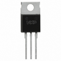
PSMN4R5-40PS,127 NXP Semiconductors, PSMN4R5-40PS,127 Datasheet

PSMN4R5-40PS,127
Specifications of PSMN4R5-40PS,127
934063908127
Related parts for PSMN4R5-40PS,127
PSMN4R5-40PS,127 Summary of contents
Page 1
... PSMN4R5-40PS N-channel 40 V 4.6 mΩ standard level MOSFET Rev. 02 — 25 June 2009 1. Product profile 1.1 General description Standard level N-channel MOSFET in TO220 package qualified to 175 °C. This product is designed and qualified for use in a wide range of industrial, communications and domestic equipment. ...
Page 2
... Figure ≤ 10 µs; pulsed °C; see °C; see Figure °C mb ≤ 10 µs; pulsed ° ° 100 j(init Ω unclamped Rev. 02 — 25 June 2009 PSMN4R5-40PS Graphic symbol mbb076 3 Version SOT78 Min Max - - 100 Figure 3 - 545 - 148 -55 175 -55 175 - 100 ...
Page 3
... T (°C) mb Fig 2. Normalized total power dissipation as a function of mounting base temperature Limit DSon Rev. 02 — 25 June 2009 PSMN4R5-40PS 03aa16 50 100 150 200 T (°C) mb 003aad297 10 μs 100 μ 100 (V) DS © NXP B.V. 2009. All rights reserved. ...
Page 4
... Fig 4. Transient thermal impedance from junction to mounting base as a function of pulse duration; typical values PSMN4R5-40PS_2 Product data sheet N-channel 40 V 4.6 mΩ standard level MOSFET Conditions see Figure Rev. 02 — 25 June 2009 PSMN4R5-40PS Min Typ Max - 0.65 1 003aad007 t p δ ...
Page 5
... D j Figure 13 MHz see Figure 14; see Figure see Figure 14; see Figure see Figure MHz °C; see Figure 0.5 Ω 4.7 Ω R G(ext) Rev. 02 — 25 June 2009 PSMN4R5-40PS Min Typ Max Unit 4 µ µ 100 100 6.7 mΩ [1] - 3.9 4.6 mΩ Ω ...
Page 6
... ° 003aad020 10 R DSon (mΩ (V) DS Fig 6. Drain-source on-state resistance as a function of drain current; typical values Rev. 02 — 25 June 2009 PSMN4R5-40PS Min Typ Max Unit - 0.75 1 003aad021 (V) = 6 100 150 200 250 I (A) D © NXP B.V. 2009. All rights reserved. ...
Page 7
... Fig 8. Input and reverse transfer capacitances as a function of gate-source voltage; typical values 003aad027 25 R DSon (mΩ 100 0 I (A) D Fig 10. Drain-source on-state resistance as a function of gate-source voltage; typical values Rev. 02 — 25 June 2009 PSMN4R5-40PS 003aad026 C iss C rss (V) GS 003aad028 (V) GS © NXP B.V. 2009. All rights reserved. ...
Page 8
... N-channel 40 V 4.6 mΩ standard level MOSFET 03aa35 5 V GS(th) (V) max − (V) GS Fig 12. Gate-source threshold voltage as a function of junction temperature 03aa27 V Fig 14. Gate charge waveform definitions 120 180 ( ° Rev. 02 — 25 June 2009 PSMN4R5-40PS 003aad280 max typ min 0 60 120 T (° GS(pl) V GS(th GS1 GS2 ...
Page 9
... Fig 16. Input, output and reverse transfer capacitances as a function of drain-source voltage; typical values 100 175 ° 0.2 0.4 0.6 0.8 Rev. 02 — 25 June 2009 PSMN4R5-40PS 003aad025 C iss C oss C rss (V) DS 003aad023 = 25 ° (V) SD © NXP B.V. 2009. All rights reserved. ...
Page 10
... 0.7 16.0 6.6 10.3 15.0 2.54 0.4 15.2 5.9 9.7 12.8 REFERENCES JEDEC JEITA SC-46 3-lead TO-220AB Rev. 02 — 25 June 2009 PSMN4R5-40PS mounting base Q c ( max. 3.30 3.8 3.0 2.6 3.0 2.79 3.5 2.7 2.2 EUROPEAN ISSUE DATE PROJECTION ...
Page 11
... Various changes to content. PSMN4R5-40PS_1 20090507 PSMN4R5-40PS_2 Product data sheet N-channel 40 V 4.6 mΩ standard level MOSFET Data sheet status Change notice Product data sheet - Objective data sheet - Rev. 02 — 25 June 2009 PSMN4R5-40PS Supersedes PSMN4R5-40PS_1 - © NXP B.V. 2009. All rights reserved ...
Page 12
... Trademarks Notice: All referenced brands, product names, service names and trademarks are the property of their respective owners. TrenchMOS — trademark of NXP B.V. http://www.nxp.com salesaddresses@nxp.com Rev. 02 — 25 June 2009 PSMN4R5-40PS © NXP B.V. 2009. All rights reserved ...
Page 13
... Please be aware that important notices concerning this document and the product(s) described herein, have been included in section ‘Legal information’. © NXP B.V. 2009. For more information, please visit: http://www.nxp.com For sales office addresses, please send an email to: salesaddresses@nxp.com Document identifier: PSMN4R5-40PS_2 All rights reserved. Date of release: 25 June 2009 ...


