STD90N02L STMicroelectronics, STD90N02L Datasheet
STD90N02L
Specifications of STD90N02L
STD90N02L
Available stocks


Related parts for STD90N02L


STD90N02L Summary of contents
Page 1
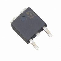
... N-channel 25V - 0.0052Ω - 60A - DPAK - IPAK STripFET™ III Power MOSFET R DS(on Max <0.006Ω 60A <0.006Ω 60A Figure 1. Marking D90N02L D90N02L Rev 4 STD90N02L STD90N02L DPAK IPAK Internal schematic diagram Package Packaging IPAK Tube DPAK Tape & reel 1/17 www ...
Page 2
... Contents Contents 1 Electrical ratings . . . . . . . . . . . . . . . . . . . . . . . . . . . . . . . . . . . . . . . . . . . . 3 2 Electrical characteristics . . . . . . . . . . . . . . . . . . . . . . . . . . . . . . . . . . . . . 4 2.1 Electrical characteristics (curves) 3 Test circuits 4 Package mechanical data . . . . . . . . . . . . . . . . . . . . . . . . . . . . . . . . . . . . 12 5 Package mechanical data . . . . . . . . . . . . . . . . . . . . . . . . . . . . . . . . . . . . 15 6 Revision history . . . . . . . . . . . . . . . . . . . . . . . . . . . . . . . . . . . . . . . . . . . 16 2/ STD90N02L - STD90N02L ...
Page 3
... STD90N02L - STD90N02L-1 1 Electrical ratings Table 2. Absolute maximum ratings Symbol (1) Drain-source voltage rating V spike V Drain-source voltage ( Drain-gate voltage (R DGR V Gate-source voltage GS (2) Drain current (continuous Drain current (continuous (3) Drain current (pulsed Total dissipation at T TOT Derating factor (4) E Single pulse avalanche energy ...
Page 4
... =10V 60A =5V GS (see Figure 17) f=1MHz Gate DC Bias =0 test signal level =20mV open drain V =10V (see Buck converter) oss gd gd. STD90N02L - STD90N02L-1 Min. Typ. Max ± 1 1.8 0.0052 0.006 0.007 0.011 Min. Typ. Max. 27 2050 =0 545 7.7 3.5 0.5 1 ...
Page 5
... STD90N02L - STD90N02L-1 Table 6. Switching times Symbol t Turn-on delay time d(on) t Rise time r t Turn-off delay time d(off) t Fall time f Table 7. Source drain diode Symbol I Source-drain current SD I Source-drain current (pulsed) SDM (1) Forward on voltage Reverse recovery time rr Q Reverse recovery charge rr Reverse recovery current ...
Page 6
... Electrical characteristics 2.1 Electrical characteristics (curves) Figure 2. Safe operating area Figure 4. Output characteristics Figure 6. Transconductance 6/17 STD90N02L - STD90N02L-1 Figure 3. Thermal impedance Figure 5. Transfer characteristics Figure 7. Static drain-source on resistance ...
Page 7
... STD90N02L - STD90N02L-1 Figure 8. Gate charge vs gate-source voltage Figure 9. Figure 10. Normalized gate threshold voltage vs temperature Figure 12. Source-drain diode forward characteristics Electrical characteristics Capacitance variations Figure 11. Normalized on resistance vs temperature Figure 13. Normalized B VDSS vs temperature 7/17 ...
Page 8
... The previous curve gives the single pulse safe operating area for unclamped inductive loads, under the following conditions: P =0.5*(1.3*B D(AVE AS(AR) D(AVE) Where the allowable current in avalanche the average power dissipation in avalanche (single pulse) D(AVE the time in avalanche AV 8/ VDSS AV AV STD90N02L - STD90N02L-1 ...
Page 9
... STD90N02L - STD90N02L-1 3 Buck converter Figure 15. Synchronous buck converter The power losses associated with the FETs in a Synchronous Buck converter can be estimated using the equations shown in the table below. The formulas give a good approximation, for the sake of performance comparison, of how different pairs of devices affect the converter efficiency ...
Page 10
... oss SW1 ------------------------------------------------- - 2 Meaning Duty-cycle Post threshold gate charge Third quadrant gate charge On state losses On-off transition losses Conduction and reverse recovery diode losses Gate driver losses Output capacitance losses STD90N02L - STD90N02L-1 Low side switch (SW2) 2 • • δ – Zero voltage switching ...
Page 11
... STD90N02L - STD90N02L-1 4 Test circuits Figure 16. Switching times test circuit for resistive load Figure 18. Test circuit for inductive load switching and diode recovery times Figure 20. Unclamped inductive waveform Figure 17. Gate charge test circuit Figure 19. Unclamped inductive load test circuit Figure 21. Switching time waveform ...
Page 12
... These packages have a Lead-free second level interconnect. The category of second level interconnect is marked on the package and on the inner box label, in compliance with JEDEC Standard JESD97. The maximum ratings related to soldering conditions are also marked on the inner box label. ECOPACK trademark. ECOPACK specifications are available at 12/17 STD90N02L - STD90N02L-1 :www.st.com ...
Page 13
... STD90N02L - STD90N02L-1 DIM TO-251 (IPAK) MECHANICAL DATA mm MIN. TYP. MAX. 2.2 2.4 0.9 1.1 0.7 1.3 0.64 0.9 5.2 5.4 0.85 0.3 0.95 0.45 0.6 0.48 0.6 6 6.2 6.4 6.6 4.4 4.6 15.9 16.3 9 9.4 0.8 1.2 0 Package mechanical data inch MIN ...
Page 14
... STD90N02L - STD90N02L-1 inch MIN. TYP. MAX. 0.086 0.094 0.035 0.043 0.001 0.009 0.025 0.035 0.204 0.212 0.017 0.023 0.019 0.023 0.236 0.244 0.200 ...
Page 15
... STD90N02L - STD90N02L-1 6 Package mechanical data DPAK FOOTPRINT All dimensions are in millimeters TAPE MECHANICAL DATA mm DIM. MIN. MAX 10.4 10.6 B1 12.1 D 1.5 1.6 D1 1.5 E 1.65 1.85 F 7.4 7.6 K0 2.55 2.75 P0 3.9 4.1 P1 7.9 8.1 P2 1.9 2 15.7 16.3 TAPE AND REEL SHIPMENT inch MIN ...
Page 16
... Revision history 7 Revision history Table 10. Document revision history Date 29-Aug-2005 07-Apr-2006 03-May-2006 24-Oct-2007 16/17 Revision 1 First release 2 New template 3 New value on Table 4, new curve 4 Corrected value on Table STD90N02L - STD90N02L-1 Changes (see Figure 14) 6, Updated BV value dss ...
Page 17
... STD90N02L - STD90N02L-1 Information in this document is provided solely in connection with ST products. STMicroelectronics NV and its subsidiaries (“ST”) reserve the right to make changes, corrections, modifications or improvements, to this document, and the products and services described herein at any time, without notice. All ST products are sold pursuant to ST’s terms and conditions of sale. ...