IRF6729MTR1PBF International Rectifier, IRF6729MTR1PBF Datasheet

MOSFET N-CH 30V 31A DIRECTFET

IRF6729MTR1PBF

Manufacturer Part Number
IRF6729MTR1PBF
Description
MOSFET N-CH 30V 31A DIRECTFET
Manufacturer
International Rectifier
Series
HEXFET®r
Datasheet

Specifications of IRF6729MTR1PBF

Fet Type
MOSFET N-Channel, Metal Oxide
Fet Feature
Logic Level Gate
Rds On (max) @ Id, Vgs
1.8 mOhm @ 31A, 10V
Drain To Source Voltage (vdss)
30V
Current - Continuous Drain (id) @ 25° C
31A
Vgs(th) (max) @ Id
2.35V @ 150µA
Gate Charge (qg) @ Vgs
63nC @ 4.5V
Input Capacitance (ciss) @ Vds
6030pF @ 15V
Power - Max
2.8W
Mounting Type
Surface Mount
Package / Case
DirectFET™ Isometric MX
Transistor Polarity
N-Channel
Resistance Drain-source Rds (on)
2.7 mOhms
Drain-source Breakdown Voltage
30 V
Gate-source Breakdown Voltage
20 V
Continuous Drain Current
190 A
Power Dissipation
104 W
Gate Charge Qg
42 nC
Lead Free Status / RoHS Status
Lead free / RoHS Compliant
Other names
IRF6729MTR1PBFTR
l
l
l
l
l
l
l
l
l
l
l
Applicable DirectFET Outline and Substrate Outline (see p.7,8 for details)
Description
The IRF6729MPbF combines the latest HEXFET® Power MOSFET Silicon technology with the advanced DirectFET
the lowest on-state resistance in a package that has the footprint of a SO-8 and only 0.7 mm profile. The DirectFET package is compatible
with existing layout geometries used in power applications, PCB assembly equipment and vapor phase, infra-red or convection soldering
techniques. Application note AN-1035 is followed regarding the manufacturing methods and processes. The DirectFET package allows dual
sided cooling to maximize thermal transfer in power systems, improving previous best thermal resistance by 80%.
The IRF6729MPbF balances industry leading on-state resistance while minimizing gate charge along with ultra low package inductance to
reduce both conduction and switching losses. This part contains an integrated Schottky diode to reduce the Qrr of the body drain diode further
reducing the losses in a Synchronous Buck circuit. The reduced losses make this product ideal for high frequency/high efficiency DC-DC
converters that power high current loads such as the latest generation of microprocessors. The IRF6729MPbF has been optimized for
parameters that are critical in synchronous buck converter’s Sync FET sockets.

ƒ
www.irf.com
V
V
I
I
I
I
E
I
Absolute Maximum Ratings
D
D
D
DM
AR
DS
GS
AS
RoHs Compliant and Halogen-Free 
Integrated Monolithic Schottky Diode
Low Profile (<0.7 mm)
Dual Sided Cooling Compatible 
Ultra Low Package Inductance
Optimized for High Frequency Switching 
Ideal for CPU Core DC-DC Converters
Optimized for Sync. FET socket of Sync. Buck Converter
Low Conduction and Switching Losses
Compatible with existing Surface Mount Techniques 
100% Rg tested
Click on this section to link to the appropriate technical paper.
Click on this section to link to the DirectFET Website.
Surface mounted on 1 in. square Cu board, steady state.
@ T
@ T
@ T
SQ
Fig 1. Typical On-Resistance vs. Gate Voltage
A
A
C
6
5
4
3
2
1
0
= 25°C
= 70°C
= 25°C
0
2
SX
V GS, Gate -to -Source Voltage (V)
4
T J = 25°C
6
Drain-to-Source Voltage
Gate-to-Source Voltage
Continuous Drain Current, V
Pulsed Drain Current
Single Pulse Avalanche Energy
Avalanche Current
ST
8
10
12
T J = 125°C
14
Ãg
g
Parameter
16
I D = 31A
GS
GS
GS
MQ
18
@ 10V
@ 10V
@ 10V
h
20
f
HEXFET
MX
30V max ±20V max 1.4mΩ@ 10V 2.2mΩ@ 4.5V
Q
Fig 2. Typical Total Gate Charge vs. Gate-to-Source Voltage
42nC
T
Repetitive rating; pulse width limited by max. junction temperature.
Starting T
V
g tot
C
DSS
measured with thermocouple mounted to top (Drain) of part.
14.0
12.0
10.0
®
8.0
6.0
4.0
2.0
0.0
MT
Power MOSFET plus Schottky Diode ‚

0
J
14nC
= 25°C, L = 0.83mH, R
Q
I D = 25A
IRF6729MTRPbF
gd
V
20
GS
MP
MX
Q G Total Gate Charge (nC)
IRF6729MPbF
4.9nC
Q
gs2
40
V DS = 24V
V DS = 15V
Max.
190
250
260
±20
30
31
25
25
R
DS(on)
G
60
40nC
Q
= 25Ω, I
rr
DirectFET™ ISOMETRIC
TM
80
AS
packaging to achieve
29nC
Q
= 25A.
oss
100
R
DS(on)
Units
V
04/02/09
1.8V
mJ
gs(th)
V
A
A
120
1

Related parts for IRF6729MTR1PBF

IRF6729MTR1PBF Summary of contents
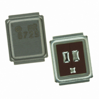
Page 1

RoHs Compliant and Halogen-Free  l Integrated Monolithic Schottky Diode l Low Profile (<0.7 mm) l Dual Sided Cooling Compatible  l Ultra Low Package Inductance l Optimized for High Frequency Switching  l Ideal for CPU Core DC-DC Converters ...

Page 2

Static @ T = 25°C (unless otherwise specified) J Parameter BV Drain-to-Source Breakdown Voltage DSS ∆ΒV /∆T Breakdown Voltage Temp. Coefficient DSS J R Static Drain-to-Source On-Resistance DS(on) V Gate Threshold Voltage GS(th) ∆V /∆T Gate Threshold Voltage Coefficient GS(th) ...

Page 3

Absolute Maximum Ratings 25°C Power Dissipation 70°C Power Dissipation 25°C Power Dissipation Peak Soldering Temperature P Operating Junction and Storage Temperature ...

Page 4

PULSE WIDTH Tj = 25°C 0.01 0 Drain-to-Source Voltage (V) Fig 4. Typical Output Characteristics 1000 15V ≤60µs PULSE WIDTH 100 150°C ...

Page 5

150° 25° -40°C 0 0.0 0.2 0.4 0.6 0.8 1.0 1.2 1.4 1.6 1.8 2 Source-to-Drain Voltage (V) Fig 10. Typical Source-Drain Diode Forward ...

Page 6

DUT 0 1K 20K S Fig 15a. Gate Charge Test Circuit D.U 20V 0.01 Ω Fig 16a. Unclamped Inductive Test Circuit ≤ 1 ≤ 0.1 % Fig 17a. Switching Time ...

Page 7

D.U.T + ƒ • • - • + ‚ -  • • • SD • Fig 18. ™ www.irf.com Driver Gate Drive P.W. D.U.T. I Waveform SD Reverse Recovery „ Current - + D.U.T. V Waveform DS Re-Applied G ...

Page 8

DirectFET™ Part Marking 8 DIMENSIONS METRIC CODE MIN MAX A 6.25 6.35 B 4.80 5.05 C 3.85 3.95 D 0.35 0.45 E 0.68 0.72 F 0.68 0.72 G 1.38 1.42 H 0.80 0.84 J 0.38 0.42 K 0.88 1.01 ...

Page 9

... IR WORLD HEADQUARTERS: 233 Kansas St., El Segundo, California 90245, USA Tel: (310) 252-7105 www.irf.com NOTE: Controlling dimensions in mm Std reel quantity is 4800 parts. (ordered as IRF6729MTRPBF). For 1000 parts on 7" reel, order IRF6729MTR1PBF REEL DIMENSIONS STANDARD OPTION (QTY 4800) TR1 OPTION (QTY 1000) ...

Related keywords